User Guides
Our User Guides provide step-by-step instructions on how to use our free online smart tools and other available software.
Find out more about the PCB Manufacturing Technology required to make a PCB.
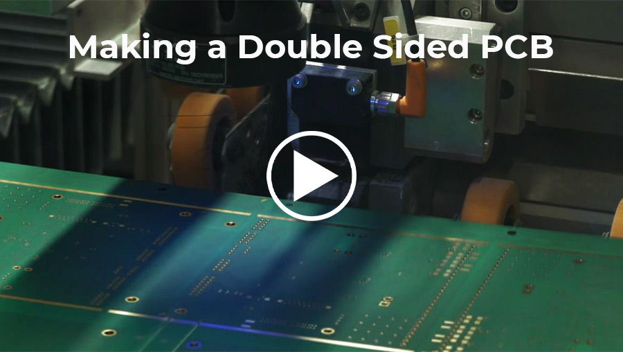
Follow the step-by-step process of making a PCB, what are the different process steps between single and double sided versus multi-layer PCB’s.
Find out more about the Galvanic process, how Via Filling is done, why do we use Direct Imaging, choosing the Right Surface Finish for your design, what about Soldermask and Legend.
Select a topic from the menu and find everything you need to know about PCB Manufacturing Technology.