
All functional circuit boards have tracks that guide electrons from one place to another in order to complete a circuit that ― hopefully! ― does what we want. These tracks have length, resistance, capacitance, and inductance with a magnitude that depends on their physical attributes, relationship to other conductive and non-conductive materials nearby, and the waveform that goes through them. DC signals and low frequency waveforms ― more accurately, waveforms with low frequency components ― aren’t affected by these properties that much, particularly if the tracks are short compared to their wavelengths. In these cases we can treat these connections as if they’re right next to each other.
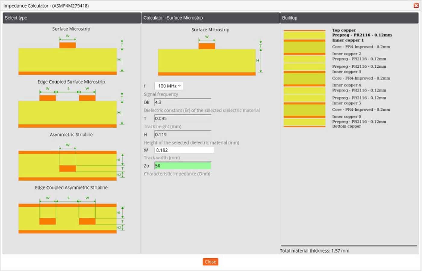
Our impedance calculator lets designers determine the correct geometry for their signals for a given buildup.
When wavelength are much shorter than the length of the track, about ¼ to ⅙ is often used, we need to start caring about the properties of the track the signal will go through. What we want is to maintain the waveform’s shape as much as possible: reduce the influence from other nearby signals and minimise reflections. For that we create a transmission line with a defined characteristic impedance, Z0, that the wavefront ― a transition between states ― ‘sees’ as it propagates along it.
A traditional transmission line is made of a track with a reference plane for a ground return. In most cases the tracks and planes will either have air or a material (FR-4, RO4350, IS400, etc.) around them with a certain dielectric constant, εr. Finally, a matching termination circuit ― usually resistors and capacitors ― need to be included in the circuit in order to prevent reflections as much as possible.
This has been an extremely short intro to a complex and extensive topic in high-frequency digital and RF design. We’ll now move on to the manufacturing part of it.
The PCB and the Circuit
For a successful high frequency design we need both the circuit to be designed well and for the circuit board to be manufactured specifically for the properties we’re after. The role of the designer is to
- define the correct geometry ― buildup, distances, and widths ― and the materials ― with their respective dielectric constants ― to create the desired characteristic impedance;
- minimise ‘interruptions’ in the transmission lines that are normally caused by vias and connectors; and,
- include an appropriate terminating circuit that reduces reflections, if needed, or plan for some form of fine-tuning after the board is manufactured.
Now comes the manufacturer’s part: manufacture the correct buildup and maintain its geometry so that the resulting transmission-line’s characteristic impedance is within a certain percentage deviation from nominal (10% is an industry standard). This is what we call defined- or controlled-impedance.
Defined Impedance at Eurocircuits
To order a defined impedance PCB start by choosing ‘DEFINED IMPEDANCE pool’ in the Visualizer (the minimum number of layers for this pooling service is four). Our handy impedance calculator then becomes available in order to calculate the geometry of the tracks that will make up the transmission lines, single-ended or differential, microstrip, or stripline for the selected buildup. It’s important to have a look at the ‘Buildup Editor’ to make sure that the buildup is as expected and that there is design data associated with each layer.
Finally, make sure to take note of the calculated ‘Total material thickness’ at the bottom right of the ‘Buildup’ section of the Buildup Editor as it will differ from the nominal thickness of the board (0.8mm, 1.2mm, 1.55mm, etc.) and that depends on the composition of the buildup.
Further information:
Be the first to read all about our news and information. Follow us on


