
Welcome to the first Engineers of Innovation BLOG.

 Who are we?
Engineers of Innovation is an alumni society of the Amsterdam university of applied sciences. The society aims to teach her members about multiple disciplines of mechanical and electrical engineering by building and competing in solar boat races. The main goal for our solar boat is that it sails as efficient as possible, this is not solely done by optimizing the drive train. There are other factors that consume power as well, like the friction with the water, peripheral electronics and the race strategy.
In this BLOG.
We will elaborate on our latest circuit board, from concept to fully assembled board, and our cooperation with Eurocircuits.
Data Logging system requirements.
Our first design is a data logging system which logs the data generated by the electronics in the boat like: the battery, MPPT’s and even the throttle. The data generated by the electronics is transmitted over the CAN bus lines so it makes sense that the datalogging system can read from the CAN bus. But there were a lot of other requirements for this design as well.
At the start of the project we had a meeting where the requirements were drafted as follows:
- Supply voltage 12 volts – 32 volts
- Can communicate over at least two separate CAN busses
- Writes to at least two SD cards for redundancy
- Communicates over internet (3G / 4G)
- GPS signal reception
- Ethernet functionality
- Wi-Fi capabilities
- Backup power supply used for safe shutdown
- Possibility to connect an LCD display
- On board IMU
Linux and communication on board.
We wanted to run Linux on the system to shorten development time when writing the software, the disadvantage here is that a lot of microprocessors that run Linux have come in a BGA package which makes them pretty hard to solder by hand. We searched online for a system on module that can run Linux, has enough I/O pins and peripherals that support CAN, MMC, UART, Ethernet, SPI, I2C, USB and an LCD. In the end we chose the Acme Acqua D36 board for use in our application.
For GPS and 3G / 4G communication we chose to use a modem in mini-PCIE form factor so we can update the modem when new functionalities like 5G are rolled out.
Schematics and Layout.
The next step in the design is drawing the schematics and selection of the components surrounding the Acqua board such as the voltage regulators, CAN transceivers and ESD protection. This part of the design takes up the most time and manpower because all parts have to be compared against each other to make sure the most efficient and best fitted part are used.
After the schematic design is complete the design has to be checked and approved by other members of the society before the process continues in the PCB design environment. The design of the PCB took a couple of nights.
First job in the layout phase is placing the components, to see where they fit best and the minimum amount of via’s is necessary in the signal traces. When the rough layout is known, the connecting traces are drawn, usually starting from the highest frequency or sensitive signal and working down to DC.
Posted below are a couple of screengrabs from the datalogging system design process. When the electrical part of the design is finished, we start with the design of the solder mask to make sure the sponsors that are helping us creating the board are on it, as well as some jokes made in those late nights of designing the board.

13-06-2018, rough component placement

21-06-2018, almost done
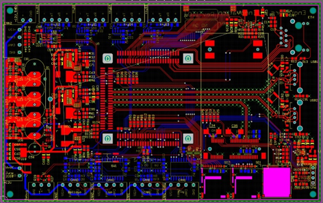
19-06-2018, halfway through
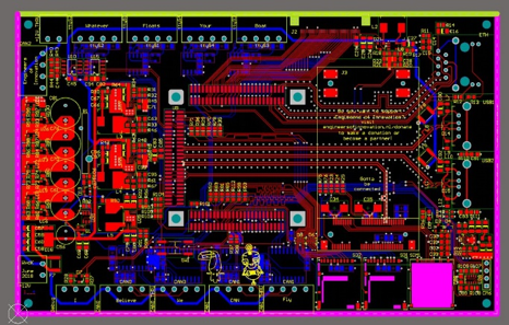
24-06-2018, checked and approved
Check and double check.
Once the design is finished, the design is checked with a design rule check program before another member of the society checks the layout to make sure it all looks alright. When the design is approved, the Gerber files are generated and uploaded in our Eurocircuits customer account.
In our online account we have a lot of options to choose from to make sure our circuit board looks and behaves the way we had in mind while designing . These options can help with the electrical characteristics of the board, like fine tuning the copper thickness of the traces to ensure the calculated impedance of our signals is exactly as we need it to be. Other options like determining the surface finish or the thickness of the solder paste stencil help us during the production process. Selecting the soldermask colour ensures that our circuit boards always look cool.

3D rendering of the circuit board in the design stage

3D rendering of the circuit board in the design stage
Populating the boards.
After the circuit boards have been received by mail we started with the component placement. For the datalogging system we only use a stencil for the top side since most IC’s on the bottom side are SOIC packages which are easy to do by hand. For the top side of the board, a stencil was used to apply solder paste. This method is faster, easier and ensures that the right amount of paste is applied to the pads. After placing the components on the board by hand the boards are placed in a reflow oven which heats up and transforms the paste into solder. When the boards are done the through hole components can be placed and the board can be tested.
When the board is completely tested the CAD files can be requested free of charge upon agreement that the files will not be used for commercial purposes in any way. More information on this can be found here.

top side of the blank datalogger(s)

bottom side of the blank datalogger(s)

The fully assembled circuit board

The finished circuit board with LCD
![]()
![]() We would like to thank Eurocircuits for making it possible for us to create systems which will help us to improve and reach our goal to sail as efficient as possible!
We would like to thank Eurocircuits for making it possible for us to create systems which will help us to improve and reach our goal to sail as efficient as possible!
Willem van der Kooij and Remco Vink
Alumnivereniging Engineers of Innovation
Weesperzijde 190, 1097 DZ, Amsterdam – website


