
We have a number of projects scheduled to be rolled out during the course of 2015. These are being developed in response to requests from our customers for more tools to help them get their designs to market faster and more reliably.
In 2015 we will launch new tools to resolve potential production issues before they delay delivery or increase costs.
We have already started to provide assembly and test solutions with our equipment range. New software tools for 2015 will help designers verify the solderability of their designs, and confirm at the design stage that the assembled boards will fit into their housings.
New services include PCB layout from schematic and BOM, semi-flex PCBs to fit electronics into complex spaces without the need for connectors, and tighter toleranced soldermasks using our new Ledia direct-imaging system.
These projects are all in the pipeline. We welcome your comments, as this might influence the order in which we will complete, test and launch them. Please leave your feedback using the voting buttons below.
Software tools:
CAM tools:
Up to now, PCB Visualizer has been an image-based tool. During 2014 we have been developing a new vector-based version. This means that the data will be composed, like Gerber, of “real” entities (tracks, pads, planes, holes etc.). This allows for faster processing, but also opens the way for a whole range of new applications and repair solutions.
- Pre-CAM data. When we prepare a job for production we run a number of routine automated procedures on our front-end engineering CAM systems ( more). These adjust the design data to our manufacturing tolerances. The procedures include
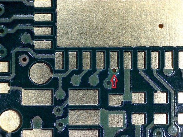
- preparing the soldermask to provide a minimum clearance from the copper pad, adequate cover over adjacent tracks, minimum webs between pads etc.(see our PCB Design Guidelines page 15)
- clipping the silkscreen to make sure that there is no ink on solderpads ( PCB Design Guidelines page 17)


- other adjustments as described in our BLOGS: Eurocircuits Data Preparation – Single Image 1 and Eurocircuits Data Preparation – Single Image 2.The Pre-CAM tool will display the results of these procedures. You can see what your finished board will look like before you place your order. If you find any potential issues, you have time to modify your design- or talk to our engineers via Online Chat.
- Pre-order solver. Our PCB Visualizer tools will continue to flag up DRC issues as they arise. The Pre-order solver software will propose possible solutions based on our service specifications and the options available in our CAM system. This may mean simply changing the classification of the job, but other options can include reducing a via-hole size, enlarging a pad size etc. Users will have the option to confirm the individual changes proposed by setting up approval rules (accept all changes, accept certain types of change, or confirm each case). The proposed solutions will be as described in our data preparation BLOGS Eurocircuits Data Preparation – Single Image 1 and Eurocircuits Data Preparation – Single Image 2
- Post-order solver. This will incorporate the present exception flow into the PCB Visualizer tool-set. The Post-order Solver will present the solutions proposed by the CAM-operator during the data preparation workflow. The user can accept or reject them. If he rejects the proposed solution he can modify his data, as at present in the case of exceptions, or he can discuss alternative solutions with our engineers via the Online Chat.
- Pre-CAM data. When we prepare a job for production we run a number of routine automated procedures on our front-end engineering CAM systems ( more). These adjust the design data to our manufacturing tolerances. The procedures include
Assembly tools:
- Solder paste editor. Edit solder paste pads on customer’s own paste layer or one generated by Eurocircuits. Functions include adding and deleting pads, as well as enlarging or shrinking them in X, Y or both. Add tooling holes or targets plus dimensions and positioning for the stencil.
- Design for Assembly. Two predictive tools to help to detect locations where there is a risk of poor soldering.
- Solder escape. Detect and flag places where solder could escape from the solder-pad, leaving a weak joint.

- Solder bridge. Detect and flag potential solder shorts based on minimum isolation distances, soldermask configuration and solder process type.


- Solder escape. Detect and flag places where solder could escape from the solder-pad, leaving a weak joint.
- 3D-DFM. “What will my assembled PCB look like?” “Will it fit into its housing?” Upload a digital BOM in EAGLE or Altium format with your PCB data-set and the 3D-DFM software will generate 3D views of your board and components with full 3D dimension data. You can then output a 3D vector file that can be input in a mechanical CAD-system, closing the gap between board data and mechanical data.
Services:
- Schematic to PCB. Supply us with the schematics + BOM (in EAGLE or Altium format). We will run BOM list analyses, place the components to your rules and lay out the board, and then produce the PCB. Each stage will include a customer approval step.
- SEMI-FLEX pool. We will offer multilayer PCBs (4 or 6 layers to be decided) with a semi-flexible 100µm FR4 core that will allow a limited number of flexings (maximum +/-25) over a radius of 4-5mm. This technology can avoid the use of connectors when fitting PCBs into complex spaces.

- High definition solder mask. We have recently installed a Ledia direct imaging machine. This exposes standard photoimageable soldermasks directly, without the need for phototools. Direct exposure allows narrower clearances between soldermask and copper pads as well as thinner webs between soldermask windows for easier and more reliable assembly of difficult components (QFN, BGA, small pitch, etc…). See our PCB Design Guidelines p. 15.


