
Input Data Requirements
Introduction
Below are the Input Data Requirements for the manufacture of PCB’s at any of the Eurocircuits production facilities.
Preferred Data input Formats
Layer Type | Preferred Formats | Accepted Alternative Formats |
| Naked CAD Files | EAGLE.BRD KiCAD | None |
| Copper Layers | Gerber X2 | Gerber X1 and DPF |
| Soldermask Layers | Gerber X2 | Gerber X1 and DPF |
| Legend Layers | Gerber X2 | Gerber X1 and DPF |
| Board Outline | Gerber X2 | Gerber X1 and DPF |
| Mechanical Layers | Gerber X2 | Gerber X1 and DPF |
| SMD Solder Paste Layers | Gerber X2 | Gerber X1 and DPF |
| Via Filling Layers | Gerber X2 | Gerber X1 and DPF |
| Carbon Layers | Gerber X2 | Gerber X1 and DPF |
| Peel-off Layers | Gerber X2 | Gerber X1 and DPF |
| Heatsink Paste Layers | Gerber X2 | Gerber X1 and DPF |
| Drill Layers | Gerber X2 | Gerber X1, XNC, Excellon 1, Sieb&Myer and DPF |
PCB Visualizer: For reasons of automated analysis and visualisation, our PCB Visualizer only accepts Gerber X2, Gerber X1, EAGLE .BRD file or KiCAD file.
For more information on the types of Input Data formats we can accept please visit our page PCB Design Guidelines – Input Data Formats.
What Data Should You Provide
If you provide Naked CAD format files from Eagle or KiCAD these should contain all the information necessary for production.
For other accepted file formats, please provide ONLY the data files that are required to produce your PCB as below:
- Copper Layers.
- Soldermask Layers.
- Legend Layers.
- Board Outline Layers.
- Mechanical Layers.
- Solder Paste Layers.
- Carbon Layers.
- Peel-off Layers.
- Via Filling Layers.
- Drill Data.
- Heatsink Paste Layers
- If you require us to prepare a customer panel (“array”, “matrix” or “biscuit”) from the single board data to your individual specification, please also provide the panel plan in either Gerber x2 or DPF format.
Please ensure that all instructions or other necessary information for the manufacture of your boards is included in the data files provided.
ONLY provide the data files that are necessary for production of your PCB.
DO NOT provide any additional files such as original CAD data (other than Eagle or KiCAD), Graphicode GWK files, PDF files, Word files (doc), Excel files (xls), etc.
Where possible check your generated output data (Gerber & Excellon files) either using our PCB Visualizer or with a Gerber viewer before you confirm your order.
Data File Names
Use clear and easy to understand file naming and try to avoid long filenames.
Make sure that we can easy determine the layer function from the filename.
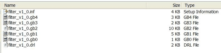
Good file naming:


File naming is too long, not advisable:

Bad file naming: no info on layer function in the file names:

Data Scaling
DO NOT scale your data.
All data provided must be at a 1:1 scale (100%).
Gerber & Excellon Files
Ensure that your Gerber files DOES NOT contain apertures with a zero-size (size = 0.00mm or inches).
Ensure that your Excellon data DOES NOT contain zero-sized tools (size=0.00mm or inches).
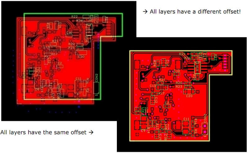
Data Offsets
Use the same origin and offset for all your layers and drill data.
Preferably use no offset at all.
Data Units
Use the same units (mm or inch) for all your output data files as used in your CAD PCB design software.
This will eliminate conversion or rounding errors.
Data Resolution
Use the same resolution (grid) for your data files to allow a perfect match.
Set the resolution (grid) for output to 6 decimals when using the imperial system and 5 to decimals when using the metric system as recommended in the Gerber specification.
If your CAD system supports only lower resolutions then use the highest available number of decimals.
Data Orientation
Make sure that your data is supplied as viewed from TOP through to the BOTTOM of the PCB.
DO NOT mirror (or reflect) any of the data layers.
Viewing a PCB from top to bottom through the board is the universal practice in the PCB industry.
We view and handle your data in that way, as does your CAD PCB design software.
This means that when viewing your Gerber data, text on the top side of your board (copper, Soldermask, legend etc) should be readable and text on the bottom side (copper, Soldermask, legend etc) should be non-readable (i.e. mirrored).

Board Identification
Add some small text (board identification, company name, etc…) in the copper layers.
Make sure the text complies with the readability rules as it will help us to avoid mirroring errors.
Board Outline
Ensure that you include the board outline on all layers.
This will enable us to properly align all layers in case of an offset problem. Also include the board outline in a separate mechanical plan data file.
Recommendations
- In your data files use flashed pads as often as possible.
- In your CAD PCB design software try to create an aperture list for data output which only shows the apertures used in the design.


