What is the Underwriters Laboratory (UL)?
The Underwriters Laboratory (UL) was set up around 120 years ago in the USA as an independent facility to test the safety of new products and new technologies. Today it has a network of sites around the world focused on product safety. It test products, certifies manufacturers, and produces and updates safety standards across a broad range of industrial and commercial sectors.
Read more about UL here.
For printed circuit boards the main standards are UL 796, the specific PCB standard, and UL 94 for flammability testing of all plastics. These specify a number of performance tests to measure the long-term reliability and fire safety of the PCB. If a board is released to these standards, it is marked with the Underwriters Laboratory logo, the manufacturers logo and the board type.
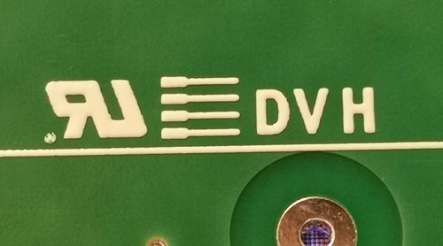
The image below shows the UL logo – Eurocircuits Trade mark – Eurocircuits UL designator – Eurocircuits factory ID.
When is the Underwriters Laboratory Marking Used?
UL marking is required whenever safety, especially flammability, is a critical issue. For European OEM’s (original equipment manufacturers) it is often required on any boards that go into equipment that will be imported into the USA. The requirement may be set by the OEM or by the end customer.
What does Underwriters Laboratory Marking Mean?
- The base material meets the specified flammability level laid down in UL94. For FR4 the level required is UL94 V0. This means that when a vertical sample of the material is introduced into the test flame and then removed, it will self-extinguish within 10 seconds and will not drip flaming particles.
All Eurocircuits FR4 materials meet the requirements of UL 94 V0. For boards requiring UL marking we use Isola and Nan Ya materials- For multilayer boards we use IS400 Mid Tg 150°C (this Tg is higher than standard FR4 to ensure full compatibility with lead-free soldering).
- For all high Tg (170° – 180° C) requirements we use Isola PCL-FR4-370-HR.
- For one and two layer boards we use IS400 Tg 150°C oder Nan Ya NP-155F Tg 150°C
=> For more information on the properties visit the UL Webseite and search for the following UL Certificates E41625 for Isola materials and E98983 for the Nan Ya material.
- The base material meets the specified level for ability to resist ignition from electrical sources. For the values see E41625 and E98983.
- The base material meets the specified electrical breakdown (tracking) or Comparative Tracking Index (CTI) value. This is the voltage difference at which the insulation properties of the base material may break down, causing safety and performance issues. The Isola and Nan Ya FR4 materials meet the requirements of Class 3 (175 – 249 V).
- The base material meets the performance profile levels specified for direct support of current carrying PCBs (DSR). These are specified in UL Standard ANSI/U/796A.
- The boards meet the other specifications set out in the table under UL marking in PCB proto, STANDARD pool and DEFINED IMPEDANCE pool below.
Eurocircuits Underwriters Laboratory Specifications
Our UL certificates E142920 can be found on our Downloads page.
Abbreviations used
- Cond = Conductor
- Edge = Please see the table and related sections below
- Thk = Thickness
- SS = One copper-clad side
- DS = Two copper clad sides including single-sided and multilayer
- DSO = Double-sided only
- Max Area Diameter: this is explained below
- Meets UL796 DSR requirement. See item 4 above
- CTI = Comparative Tracing Index. See item 3 above
TIPS
- UL marking is free of charge.
- To add UL marking to your order, click on “Advanced options” section in the PCB Configurator and then select the “Yes” next to the “UL marking” option.
- When data has been uploaded, the Marking editor can be used to define the UL logo position.
General
- We offer UL marking in PCB proto, STANDARD pool, DEFINED IMPEDANCE pool and HDI pool only.
- All boards requiring UL marking are either made in our factories in Eger, Hungary or Aachen, Germany.
- Active board classes, each with its own UL marking:
- Eger, Hungary – Factory ID is H
- Multilayer boards: designator ML; marking:

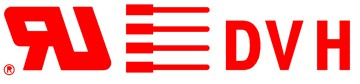
UL ML - 1- and 2-layer boards: designator DV; marking:
UL DV
- Multilayer boards: designator ML; marking:
- Aachen, Germany – Factory ID is G
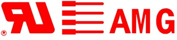
- Multilayer boards: designator AM; marking:
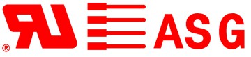
UL ML - 1- and 2-layer boards: designator AS; marking:
UL DV
- Multilayer boards: designator AM; marking:
- Eger, Hungary – Factory ID is H
The other classes listed in the certificate are no longer used.
IMPORTANT
- UL marking is only available for PCBs which conform to the required parameters.
Additional technologies overview
Technology
|
ML H / AM G |
DV H / AS G |
| Carbon ink (contact) | No | No |
| Via fill with resin | Yes | Yes |
| Peelable mask | Yes | Yes |
| Plating finishes: HAL PbSn HAL Sn Immersion NiAu (ENIG) Immersion Ag |
Yes Yes Yes Yes |
Yes Yes Yes Yes |
| Soldermask:
Green/Red/Blue/Black/No White/Transparent/PixtureBlackWhite |
Yes
No |
Yes
No |
| Edge Connector Gold | Yes | Yes |
| PTH on the board edge | Yes | Yes |
| Round-edge plating | Yes | Yes |
| Copper up to board edge | Yes | Yes |
| Heatsink paste | No | No |
If you have any questions, please contact us by email at euro@eurocircuits.com or use our online Chat.