Eurocircuits data preparation – Single Image (part I) – drill data and copper image
Have you ever wondered what we are doing to your data when the order status is Single Image? Here is the answer based on the instructions we give to our data preparation engineers. Many of the steps described below are automated for speed and accuracy but we have ignored this to make a clearer presentation. More information on our requirements can be found on the home page under “Technology Guidelines”.
Stage 2 – Single Image data preparation (Single Image and Single Image Cross Check)
The name “Single Image” may be slightly confusing as it includes both single circuits and customer panels or assembly arrays. We use it to mean what we will deliver to the customer (individual circuit or panelised array) in contrast to our pooled production panels.
Build the job
- load the job data received from Stage 1 (Analysis of PCB CAD data)
- remove everything outside the board outline.
- build a job netlist from the drill and Gerber data. We will use this later to check that we have not made any mistakes during the data preparation. If you have supplied an IPC netlist from your CAD system we will check the job netlist against this at this stage and raise an exception if we find discrepancies.
- save a copy of the layers as received as a reference for later checks.
- load the correct build-up for the job using the material thickness/copper thickness etc specified in the order
- save the job.
Prepare the drill layer(s)
- calculate the Nominal Hole Size. Where our standard tolerances (+/- 0.1 mm) apply, the nominal hole size is the finished hole size specified in the data (e.g. 0.80 mm). Where the designer has specified his own tolerance (e.g. +0.1/-0.00) we will aim to produce a hole in the middle of this tolerance band (so the Nominal Hole Size will be 0.85 mm).
- increase the Nominal Hole Size to the Production Hole Size to accommodate the plating on the hole walls, the mechanical tolerances of the drilling machines etc. This is to ensure that every finished hole size is within tolerance. The rules are:
- plated holes with finished diameter of 0.45 mm or less (taken to be via holes): increase by 0.1 mm.
- plated holes with finished diameter of 0.50 mm or more (taken to be component holes): increase by 0.15 mm.
- non-plated holes: increase by 0.05 mm. This is due to the bounce-back of the laminate: the drilled hole is always slightly smaller than the drill diameter.
- Sort and regroup all drills and slots in the correct functional drill layer.
- Put all drill and slots – PTH and NPTH – to the first drill run
- Move any NPTH drill, slot or inner cut-out that is or can be seen as part of the board profile to the profiling run.
- Move all NPTH drills larger then 6.00mm to the profiling run.
- Move all NPTH drills and slots that are in a copper area (pad or plane) to the second drill run or the profiling run as per production requirements.
There are 3 possible steps in the production flow where we can drill holes:
- First Drill Run or plated drill layer:
-
- This is one of the first steps in production. All holes drilled here will become plated (PTH) unless the hole is being covered with dry film, this process is commonly known as “tenting” or “tented NPTH hole”. Tented NPTH holes MUST have a copper clearance of 0.30mm and can have a maximum size of 6.00mm.
-
- Second Drill Run or non-plated drill layer:
- Is performed after the electroless plating process (or blackhole process). All holes here are non-plated (NPTH)
- Profiling run or rout layer:
- Is the last step where the profiling of the board is done. These holes are also non-plated (NPTH)
Outer Layer preparation
- Clean the data
- Replace any painted pads and areas with proper flash pads and polygons. Painted features filled with small draws were common in old-fashioned standard Gerber data but are not needed with Extended Gerber where you can define any pad shape or filled area you require.
Check for missing copper pads on plated-through holes (PTH).
- Check non-plated holes (NPTH)
- Any NPTH hole which has a copper pad that is smaller than the hole, remove the copper pad
- For the NPTH in the first drill run (Tented NPTH): Check the drill to copper clearance, it should be minimal 0.30mm.
- Repair if needed by creating 0.30mm clearance to copper (=same repair methods/restrictions as Minimum copper to edge clearance in DRC – see article about Data Analysis)
- If impossible to repair then move the NPTH to the second drill run or the profiling run as per production requirements.
- Check and repair the copper free area of 0.25mm for all elements from the rout layer (=same repair methods/restrictions as Minimum copper to edge clearance in DRC)
- Run automated design-rule checks (DRCs) to find violations against the minimum required design specifications of the chosen service. At this stage, any violation found should normally be repairable by us.
- Check and repair minor copper defects which may cause problems in production: peelables (see PCB Design Guidelines – Copper Layers), pinholes and copper slivers:
-
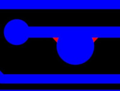
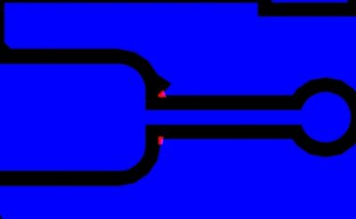
- The dimensional values of the copper defects to be detected depend upon the pattern class – Peelables and Pinholes are filled, Slivers are removed.
- Save the job.
Inner layer preparation
- Clean the data as for outer layers.
- Remove all non-functional pads
-
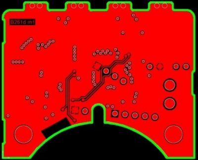
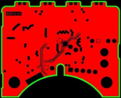
- Check for missing copper pads on connected plated-through holes
- Check and repair the copper free area of 0.25mm for all elements from the rout layer (=same repair methods/restrictions as Minimum copper to edge clearance in DRC).
- Check and repair all thermal pads as needed
-


- Check for proper thermal to plane connections, rotate the thermal if needed – Min thermal “air-gap” should be 0.20mm.
- Run automated design-rule checks (DRCs) to find violations against the minimum required design specifications of the chosen service. At this stage, any violation found should normally be repairable by us.
- Save the job.

