How Often Can You Raise a Eurocircuits PCB to Lead-free Soldering Temperatures?
By Dirk Stans – Eurocircuits and Geert Willems – Center for Electronics Design & Manufacturing, imec
References.
[1] PBA Design-for-Manufacturing Guideline EDM-D-001: PCB Specification, imec-cEDM, July 2013.
[2] IPC-4101C: Specification for Base Materials for Rigid and Multilayer Boards
[3] Geert Willems, Piet Watté, Predicting PCB delamination in lead-free assembly, Global SMT &
Packaging, Vol. 10, No. 9, September 2010, p. 10.
Situation today!
- We live in the lead-free soldering era
- Soldering temperatures are between 235°C and 250°C (+25-35°C)
- Our many years of experience with lead-free soldering of FR-4 boards has revealed advantages and disadvantages
- The quality and reliability of your product is critical for its success in the market-place
- These factors make the choice of PCB laminate base materials increasingly important
- But how do you as a PCB designer make an informed choice?
- And how can you design robustness into your PCB to ensure optimum quality during assembly and reliability during the whole envisaged product lifetime?
First reaction!
There are a host of material parameters to consider for the current generation of PCB designs:
- T260, T288
- CTEz
- Td
- Tg
- Moisture absorption
They determine whether or not your PCB will delaminate and the vias will survive the lead-free assembly conditions applied to your PCB.
How do you select the right combination for your design?
One could select the best possible value for each parameter but this limits the number of available materials considerably. Furthermore, these materials have their own disadvantages such as a poor manufacturability and brittleness.
What are the consequences? Is your problem solved?
- If you select non-standard materials with unnecessarily high thermal performance requirements a way too expensive PCB is the result.
- Your board supplier may not stock the material you have specified.
- The material manufacturer may cease production of less frequently used materials.
Your PCB supply is expensive and not future safe.
To provide a cost effective and scientifically sound solution to its customers Eurocircuits partnered with imec’s Center for Electronics Design & Manufacturing. The methodology presented here is described in detail in PBA Design-for-Manufacturing Guideline: EDM-D-001: PCB Specification, developed by imec/cEDM and available at www.cedm.be. Parts of the guideline are reproduced here with permission of imec/cEDM.
Better start from what you know and can control!
Your product will be soldered lead-free so you need lead-free soldering compatible FR-4. The requirements for the PCB laminate depend on:
- How many times your PCB will be raised to lead-free soldering temperature during fabrication and assembly or “how many soldering cycles will your board need for assembly and possible repair?”.
- The maximum operating temperature for your application.
- The planned lifetime of your application counted in number of thermal cycles.
Your internal or external assembly partners should be able to provide the answer to the first question. Your customer or the end-user is the source to find the answer to the other questions.
Possible fabrication and assembly soldering cycles
How to determine the number of soldering temperature cycles to a PCB? The answer is given in the table below, Ref. [1].
The PCB fabrication and assembly processes given in the first column determine the number of solder cycles to be taken into account.
| Process | Cycles | Explanation |
| HAL lead-free (bare board) | 2 | One HAL dip + one extra dip |
| Reflow | 1 | |
| Wave soldering | 1 | |
| Selective soldering | 1 | Including manual soldering |
| Touch-up / repair | 1 | Removing shorts or opens on leaded components |
| Component replacement | 3 | Removal+clean+re-solder: valid for using local heating |
Specifications of lead-free soldering compatible FR-4
Always start from an internationally accepted standard. The IPC standard that defines lead-free solderable FR-4 is IPC-4101C:
- There are 14 classes of lead-free compatible laminates: /99, /101, /102,/103[WG1] ,/121,/122, /124, /125/126,/127,/128,/129,/130,/131, each with slightly different properties.
More detailed information can be obtained via www.ipc.org
- Key parameters:
- Decomposition temperature: Td (Thermal decomposition temperature: see further)
- Time-to-delamination: T260, T288, T300 (Time to delamination at 260°C, 288°C and 300°C; see further down)
- Z-expansion (thickness direction): coefficients of thermal expansion alpha 1 and alpha 2 (ppm/oC), and CTEz the z-expansion in % between 50oC and 260oC
Rather than specifying a base material to your PCB supplier, check that his materials conform to one of the IPC defined classes and see what minimum values he guarantees for these key parameters. Your boards will be cheaper and available faster.
Let”s compare the SnPb era FR-4 against the lead-free compatible FR-4 in respect of these key parameters.
Typical values of SnPb-era FR4 laminate materials compared to those of the lead-free compatible FR4 classes .
|
FR4 SnPb |
99 |
101 |
121 |
124 |
126 |
129 |
122 |
125 |
127 |
128 |
130 |
131 |
|
|
Td (°C) |
+/-300 |
325 |
310 |
310 |
325 |
340 |
340 |
310 |
325 |
310 |
325 |
340 |
340 |
|
T260 (min) |
2-15 |
30 |
30 |
30 |
30 |
30 |
30 |
30 |
30 |
30 |
30 |
30 |
30 |
|
T280 (min) |
>10 sec |
5 |
5 |
5 |
5 |
15 |
15 |
5 |
5 |
5 |
5 |
15 |
15 |
|
CTEz (%) |
+/-4.5 |
3.5 |
4.0 |
4.0 |
3.5 |
3.0 |
3.5 |
4.0 |
3.5 |
4.0 |
3.5 |
3.0 |
3.5 |
As the table shows, there are significant differences between older FR4 and current lead-free solderable FR4s (shown in IPC classes) for the key parameters Td, T260, T288 and CTEz.
We now solder 25-35°C hotter than in tin-lead solder times. This causes risks for:
- Delamination: parameters T260, T288 and to a lesser extent Td.
- Via cracks: parameter CTEz
Let”s further examine the effect of these parameters.
Delamination
- Driving force:
- Laminate decomposition
- Moisture within the PCB[1]
- Key parameters:
- Time-to-delamination: T260 – T288 – T300
- Decomposition temperature Td
- Failure types
- “blisters”
- High Ohm resistance shorts
- Track failure (open circuit)
- Via cracking (open circuit)
- Field failure (usually not detectable during PCB assembly testing).
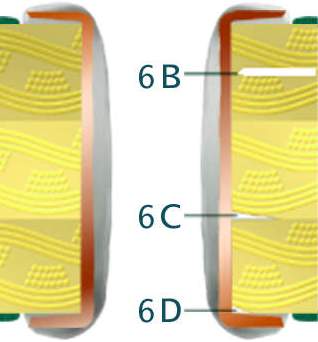
Delamination (extended separation inside the PCB)
Not more than 25 % of the distance between adjacent conductors or plated-through holes.
Not more than 1% of the printed wiring area on each side may be affected.
No propagation as a result of thermal stress testing or representative condition.
(6A) shows separation between two glass weave layers in the base material. The separation can also occur between the base material and the copper foil.
(6B) shows a separation between individual layers.
(6C) and (6D) show separations between laminate and internal or external pads respectively, or copper planes.
Key specifications of FR-4 with respect to temperature behavior
- Decomposition temperature – Td
- Measured using TGA: Thermo-Gravimetrical Analysis
- The decomposition temperature Td determines how fast your board starts to degrade during heating. On reaching the Td temperature after heating up at a speed of 10°C/min, 5% of the base material will be decomposed. Since lead-free soldering needs temperatures about 25°C hotter than before, we need Td values for our material that are higher than before.
- Time-to-Delamination: T260-T288-T300
- Measured using TMA: Thermo-Mechanical Analysis
T260-T288-T300 determine how long your base material can resist these temperatures before the material starts to delaminate (the material will increase in thickness).
- Measured using TMA: Thermo-Mechanical Analysis
Cycles to delamination as a function of laminate properties
Research and modeling by imec-cEDM has proven, Ref. [1, 2], that the IPC /sheet boundary conditions – especially the fixed T260=30min does not provide sufficient protection to delamination. The following IPC-4101 compatible definition of thermal performance classes guarantees the indicated number Nd of solder cycles without cohesive[2] delamination, Ref. [1]. Note the more stringent T260 and T288 requirements.
|
Category |
Td (°C) Min. v |
T260 (min) Min. v |
T288 (min) Min. v |
CTEz (%) Max. v |
Nd |
Potentially compliant IPC-4101 sheet numbers |
|
Basic |
310 |
30 |
5 |
4 |
7 |
99, 101, 102, 103, 121, 122, 124, 125, 126, 127, 128, 129, 130, 131 |
|
Mid |
325 |
50 |
10 |
3.5 |
12 |
99, 102, 103, 124, 125, 126, 128, 129, 130, 131 |
|
High |
340 |
80 |
15 |
3 |
20 |
102, 126, 130 |
A mid performance material with a T260=50min and a T288=10min will be able to withstand at least 12 solder cycles before delamination will occur in the bulk of the laminate assuming the PCB is dry. The physico-chemical mechanism links Td, T260 and T288. Therefore, the actual Td value is not an additional parameter.
Graphs to determine the number of solder cycles to delamination for a given combination of Time-to-delamination and decomposition temperatures are given respectively in EDM-D-001 and Ref. [2]. A calculation tool is available at www.cedm.be (free use for cEDM members).
Via cracking
A via crack is usually caused by the difference in thermal expansion between the laminate and the copper barrel of the hole. This is influenced by the thickness of the board, the thickness of the copper plating and the diameter of the hole. The key material parameters for this is the CTEz value.
- Driving force:
- Difference in CTE between the laminate and the copper plating of the via.
- Key parameter:
- CTEz: 50-260oC. The higher the expansion the worse the situation is.
- (Tg, a1, a2) (Explanation further down in the text)
- Failure types
- Apparently open solder joint (especially BGA)
- Intermittent open connection
- Open via connection
- Field failure (often not testable during manufacture)
- Reduced PCB lifetime
Via cracks due to thermal stress can appear during soldering or during the operation of the board. Soldering stress cracks are tested by repeated soldering and for operational lifetime one tests this effect through accelerated thermal cycling testing (typical -40oC/125oC).
Let’s concentrate on the most critical effect of temperature cycling: z-axis tension in the via barrel due to the much larger Coefficient of Thermal Expansion CTE of the laminate in the z-axis compared to the CTE=17ppm/oC of copper.
CTEz, a1, a2: expansion in z-direction
The material parameter that has the biggest impact on cyclic tension in the z-axis direction is the CTEz value.
In the graph above you can see the relationship between the z-axis expansion of the material (CTEz) and temperature. The expansion is a rather linear process but has a click point where the angle of the curve changes and the z-axis expansion increases faster per °C. This click point is at the Tg value of the base material. It is actually the way the Tg is determined using Thermo-Mechanical Analysis (TMA).
The graph also shows that a traditional FR-4 material with Tg=150°C (orange line) has a CTEz value which is a lot higher than for the new lead-free solderable material (light green line) with the same Tg value. This is achieved by reducing the CTE of the laminate through the use of inert fillers (increases drill wear!) or/and using higher functionality epoxy types (harder, more brittle materials).
Conclusion: CTEz is far more important than Tg with respect to z-axis expansion. A higher Tg material does not guarantee a higher thermal performance with respect to lead-free soldering. However, it will increase the PCB cost.
Via crack model
According to EDM-D-001, 4.4.3, Ref. [1], plastic via deformation dominates under soldering conditions. Therefore, the via lifetime (number of solder cycles to failure) depends mainly on the CTEz value of the laminate. The small dependency on the via dimensions can be neglected for specification purposes. EDM-D-001 provides CTEz based criteria for selecting laminates that will provide sufficient number of solder cycles to via failure.
Eurocircuits materials with a maximum CTEz=3.5% guarantee conservatively less than 1% via failure after 14 solder cycles.
Note that under soldering conditions the vias are stretched by several percent which is a very large mechanical load knowing that via barrels will immediately fail when stretched by 7 to 10%, Ref. [1], Appendix B.
Via: operational reliability – number of -40/125oC cycles to via-failure
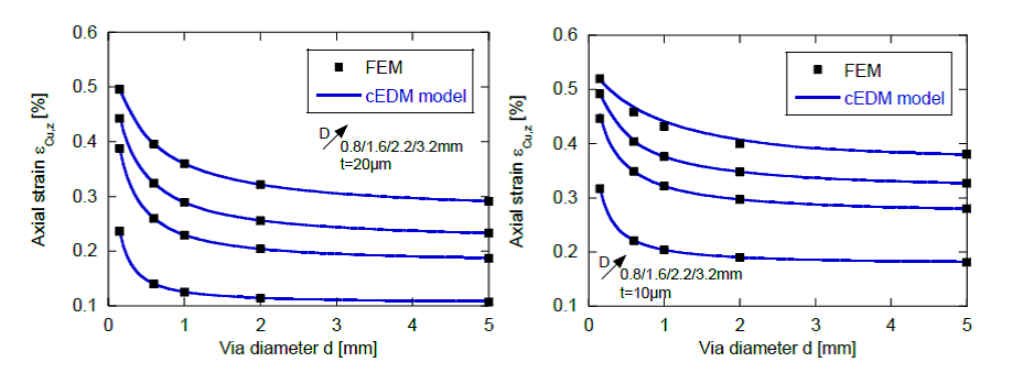
Under operational conditions the dimensions, board thickness and plating thickness may have a significant impact on the lifetime. In general the stress increases and thus the lifetime decreases with increasing board thickness, decreasing via diameter and decreasing plating thickness. Imec/cEDM developed an accurate analytical model to calculate the via strain during thermal cycling and to estimate the via lifetime.
The graphs below show the dependency of the via strain under -40/125oC cycling for a laminate with a1=50ppm/oC, an board thickness D and via diameter d for t=20µm (left) and t=10µm (right) via plating. (FEM: numerical Finite Element Modeling results)
Using the Wöhler relationship which relates the number of cycles to failure to the cyclic strain on the vias the lifetime of the vias under different operational conditions can be calculated. An online via lifetime calculation tool is available at www.cedm.be (free for cEDM members). An offline version for embedding in PCB design tools is available from imec/cEDM.
Impact of soldering on the life expectancy of the PCB: via degradation
As mentioned before soldering imposes very large stresses on the vias. When the via does not fail during soldering – which is off course the intention – the lifetime of the PCB vias is reduced after soldering compared to the lifetime of vias of an unsoldered board. EDM-D-001 explains how this effect can be calculated. Again, selecting materials with a low CTEz reduces the impact of the soldering on the via lifetime.
If we look again at our standard value CTEz of 3.5% we achieve less than 4.6% loss of life expectancy per applied solder cycle, EDM-D-001, 4.4.4, leading to an overall lifetime reduction for an unrepaired PBA between 13 to 20%.
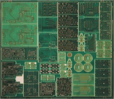
Eurocircuits pooling panels.
The vast majority of our orders are produced on pooling panels.
The standard technological values for these boards are:
– board thickness 1.6mm
– minimum track & gap 150µm
– smallest hole size 0.25mm
– minimum copper plating in the holes 20µm
Based on these values and imec/cEDM’s methodology described in Ref. [1] and explained above, we have determined specifications for the base material we use.
Our goal is to offer our customers a guaranteed performance for our PCBs during their assembly processes and sufficient PCB reliability for medium operationally stressed electronic assemblies.
How often may you heat up your PCB to soldering temperature?
- Pooling – minimum material specifications and maximum number of solder cycles
- T260 = 60min, T288 > 10min & Td = 325°C =>16 cycles
- CTEz = 3.5%
- 1.6mm PCB => 14 cycles 1% failure or 11 cycles 0.1% failure
- 20µm plating
- Tg 145°C=> max operating temp 120°C
- Eurocircuits wants to be on the safe side => -2 cycles
- Lead-free hot-air solder-leveling involves => -2 cycles
- So, using our minimum guaranteed material specification, a standard Eurocircuits pooling PCB with lead-free HAL finish may be raised to the lead-free soldering temperature (=<260°C) during assembly 10 times – on condition that the PCB is sufficiently dry[3].
- The PCBs maximum operational temperature is 120°C.
- In fact, the materials we currently use, Isola IS400 and Nan Ya NP-155F, perform much better than our minimum guaranteed specifications. They have the values: T260=60 minutes, T288>10 minutes, Td=350°C, CTEz=3%, Tg=145°C. CTEz=3% would bring the basic number of solder cycles already to 20 with 1% failure instead of 14 cycles.
- Via reliability decreases over time and with every applied solder cycle (for example, 8 cycles at 4.6% adds up to +/-37% loss of life expectancy).
- For better reliability use large vias and limit board thickness. The laminate CTEz and the CTE below Tg a1 are the dominating via reliability parameters.
“hot” – “hotter” – “hottest”
Like any good steak, any good PCB can be burned!
This article is made with the support of:
Imec’s Center for Electronics Design & Manufacturing
Kapeldreef 75
3001 Heverlee
Belgium
Geert Willems – 0498 919464 – Geert.Willems@imec.be
[1] Moisture absorbed into the PCB can exacerbate delamination and, due to the higher soldering temperature, has become a much more critical parameter than it was with SnPb solder. It can be countered by storing PCBs in a temperature and humidity controlled environment. As moisture, if present, would be a local variable, we have not considered it further in our discussion of material properties.
[2] Cohesive delamination: delamination in the bulk of the laminate as opposed to delamination at the resin/copper interface.
[3] Moisture absorbed into the PCB increases the tendency to delamination due to the additional internal stress of the water vapor pressure. This can be countered by storing PCBs in dry bags or low humidity (<5 RH%) dry cabinets.


