The Function of Beautiful

When we say functionality during electronics development we normally mean electrical functionality: the circuit that controls the flow of electrons to convert incoming inputs into desired outputs. The look of this functionality doesn’t normally come into it as it is often considered superfluous. I argue, though, that the beauty of electronics is functionality in many applications, and by beautiful, I usually mean a combination of aesthetics, symmetry, neatness, and having elements of good user experience.
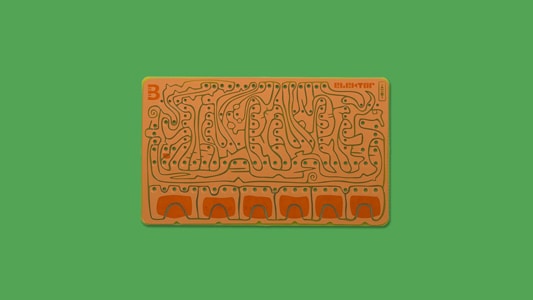
Take projects that aim to be educational. Having something pleasing to the eye attracts those who are new to or curious about our craft, much more so than a dull piece of traditional all-too-rectangularly-green PCB. This becomes obvious when we consider the warm reaction to organic-looking hand-drawn electronics from the 1960s and 70s, even from experienced engineers; these circuits are immediately engaging and relatable because of how they look, while what they do electrically is not as important. (I’ve been told by quite a few people that my own organic-like artistic designs helped professional engineers and makers get their partners to become more interested in their work).
At trade-shows or online we’d like our products to stand out. If that’s the goal, then beauty and uniqueness is a function of the electronics: to get people to interact at the booth or on social media. Same for demo-, eval-, and dev-boards. Their primary function is to entice people to actually use them, which is more likely to happen if they are aesthetically engaging, unique, easy to use, and… fun. As a bonus, we benefit from people sharing pictures of these boards on social media and with their colleagues back at work, rather than put them in a drawer to be forgotten until obsolescence.
Paying attention to looks and usability such as rounded corners, indentations to hold the board, symmetry, and thoughtful component placing reflects that there’s likely similar attention given to the electrical functionality. A beautiful circuit often means that the designer was able to take the time to consider more than the bare minimum; it signals mastery of the craft. Going through the thought process of how the end-user perceives and uses the board allows us to look at what we’re working on from a different perspective. This is always a good thing; it helps us discover problems or creative solutions for things such as placement and routing issues.
Contrary to what it may seem at first, making a circuit beautiful doesn’t necessarily have to cost more to manufacture. The router bit that cuts the board from the panel doesn’t care if the outline is curved. The masks don’t care if there’s an elaborated design on them; they’re capable of any shape, not just the 135-degree routing turns or rectangular and circular shapes that EDA tools have trained us to use.
I’ve designed many beautiful and functional boards. My approach is to consider both the aesthetics and the electrical functionality as having equal importance, as they are much of the same. The results of this approach can be superior to designing while aesthetics and functionality are separated, ‘forced’ together at the end.
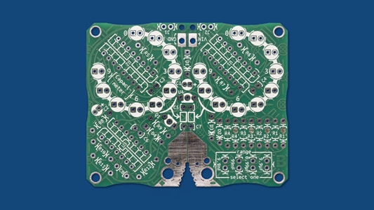
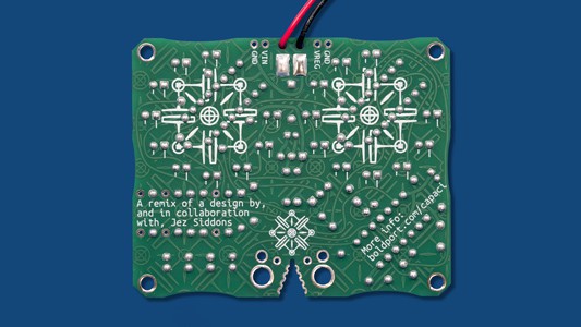
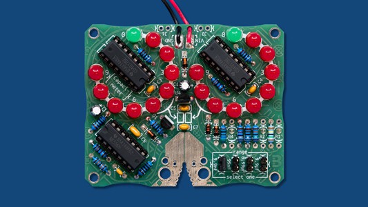
As an example here’s ‘Capaci-meter’ which I designed, based on a circuit by Jez Siddons. You can see the outline dimples to guide fingers for where to hold the board. There are strain relief holes for the battery contact cables. The legend of the jumpers on the top side’s bottom right gives the user enough cues so they don’t need to refer to the documentation. (Images courtesy of Boldport.)
Why not try it?
Adding aspects of aesthetics to our boards may not be simple and straightforward due to the way EDA tools work, but it does not have to be elaborate to be effective.
Start by imagining the end result and how you’d want the user to experience the board, perhaps by sketching concepts in a notebook for faster iteration. Also do the same while choosing components and then when placing them. Choose LED colours that match the theme of the board; create helpful legend so the user doesn’t need to consult a manual; round sharp corners; add strain relief for cables; create smooth cutouts for where fingers might go when users hold the board, etc. Be as creative as you are with the electrical design and layout (it is creative work too!). If you work with industrial designers, consult them from the beginning and work with them during development; they’ll appreciate it and your product will be better with fewer, and perhaps quite costly, late-stage modifications.
You may read this and think that this only applies to designs that are exposed, like soldering kits. But even PCBs that are enclosed get noticed if they’re special in any way. They are sometimes used for marketing and promotions. Even simple things can get attention, like a thoughtful feature, special messages, interesting colours, and unique components and techniques. If you try something new, let us know!
In the ‘Pease’ board I’ve put the schematic in silkscreen and added a ruler for good measure. (Images courtesy of Boldport.)
Bring your product to market on time and within budget – join the Eurocircuits Community


![]()

