User Guides
Our User Guides provide step-by-step instructions on how to use our free online smart tools and other available software.
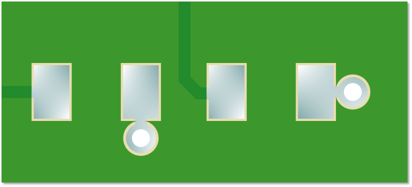
Solder Escape/Wick (also known as Solder Drainage) is where the Solder flows away from the SMD Pad towards a connected copper element, usually Via Hole. However, it may also be a copper pad or area that is not covered or isolated with Soldermask.
If a Via Hole is too close or inside an SMD pad, the heat dissipation and surface tension (the meniscus effect, capillary action) may cause the Solder to flow towards the hole and away from the SMD pad.
This would then result in either a poor quality or even dry solder joints.
Simply increasing the volume of the Solder Paste may sound like a solution but it results in either, other SMD Pads having too much Solder Paste or the need for, stepped solder paste stencils, larger pads or larger solder paste apertures in the stencil, all of which are undesirable.
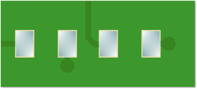
Below is a graphical representation of what happens to the Solder during the Reflow process if the Via Hole is too close to an SMD pad and there is no Soldermask web/dam between them.
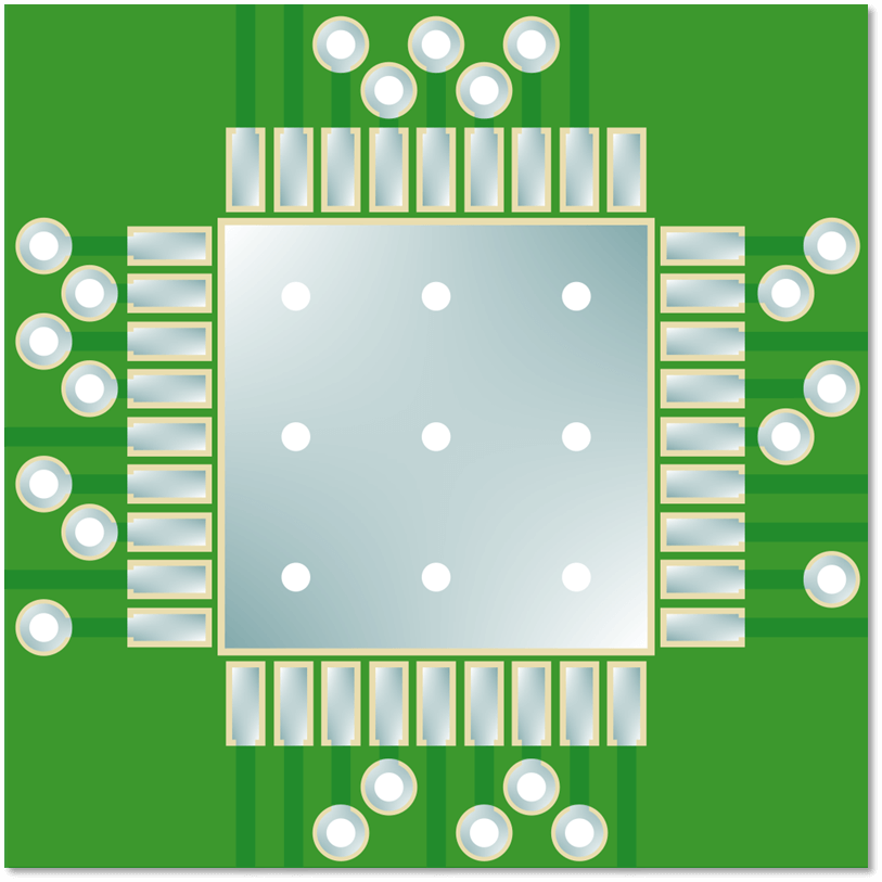
Via Holes that have been placed too close to a SMD pad with No Soldermask web/dam.
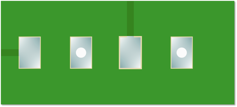
By using the Via fill with resin technique it ensures that the Via Hole is fully covered with Soldermask and this stops the solder flowing away from the SMD pad.
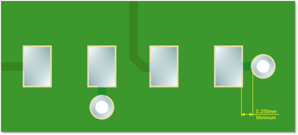
It should be noted that there are various articles that discuss how far a Via should be from a SMD pad, however, the consensus seems to be a minimum of 0.250mm from edge of the SMD pad to the edge of the Via pad.
It is also important that by moving the Via to meet this minimum distance also allows for a Soldermask web/dam between the SMD pad and the Via.
As miniaturisation of electronics continues Via Holes in SMD pads is seen as a solution to gain more real estate on PCB’s. The problem is that Solder will flow from the SMD Pad into the Via Hole resulting in a dry or weak Solder joint of the SMD pad.

It should be noted that there are various articles that discuss how far a Via should be from a SMD pad, however, the consensus seems to be a minimum of 0.250mm from edge of the SMD pad to the edge of the Via pad.
It is also important that by moving the Via to meet this minimum distance also allows for a Soldermask web/dam between the SMD pad and the Via.


By using the Via Fill with resin technique it ensures that Via Holes are either covered fully with Soldermask or copper/final finish ensuring the Solder will not flow into the Via Hole.
It has become quite common for IC chip manufacturers to use the body as either a ground connection or as a way to dissipate heat or both.
To achieve this they recommend a copper area under the IC main body with a matrix of Via Holes.
The problem is the body must be soldered to this copper area and if there are open Via Holes then the Solder will escape into them and may result in a poor/weak/dry Solder joint and without X-ray inspection impossible to verify the quality of the solder joint. .
IC chip manufacturers suggest using Soldermask around the Via Holes or tenting them to stop the Solder escaping.
Whilst this sounds practical it has disadvantages, both methods reduce the area of the IC that can be soldered. This may affect the quality of the ground connection or the effectiveness of the heat dissipation.
In reality using Soldermask to stop the Solder escaping is not a practical solution in this type of design.

The only real solution is to use Via Fill with resin which will allow for the IC body to be correctly soldered to the copper area and thus provides the most effective solution.