User Guides
Our User Guides provide step-by-step instructions on how to use our free online smart tools and other available software.
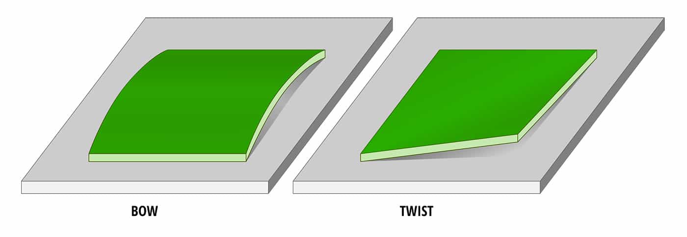
The IPC-TM-650 defines bow and twist as follows:
“Bow (Sheet, Panel, or Printed Board): The deviation from flatness of a board characterized by a roughly cylindrical or spherical curvature such that, if the product is rectangular, its four corners are in the same plane.” “Twist: The deformation of a rectangular sheet, panel, or printed board that occurs parallel to a diagonal across its surface, such that one of the corners of the sheet is not in the plane that contains the other three corners.” These definitions apply to panels or individual PCBs; in this article we’ll use ‘PCB’ to include panels. Bow and twist against a flat reference plane. The IPC also sets the acceptability criteria in its IPC-6012: “maximum bow and twist of 0.75% for printed boards that use surface mount components and 1.5% for all other printed boards”. It adds that the ‘end products’ should be assessed in ‘delivered form’ which means that the measurements for acceptability is done after all manufacturing and assembly steps are complete. For more complicated cases, such as for odd shaped boards, the IPC suggests AABUS: as agreed upon between user and supplier.
During manufacturing, any deviation from perfectly flat may introduce misalignments when mounting on machines.
During component assembly, the flatness of the PCB is important for accurate solder paste dispensing, automatic board transport on the production equipment, and during component mounting. It’s easy to imagine that any distortion such as a bow or twist in the PCB could cause minute, but impactful, misalignments when we’re placing tiny components such as 0402s. Or, the board might get stuck in a transport belt or loader or unloader and block the production line.
During use, bow and twist could make fitting the PCB into an enclosure, or applying fasteners such as screws, difficult or even impossible in extreme cases.
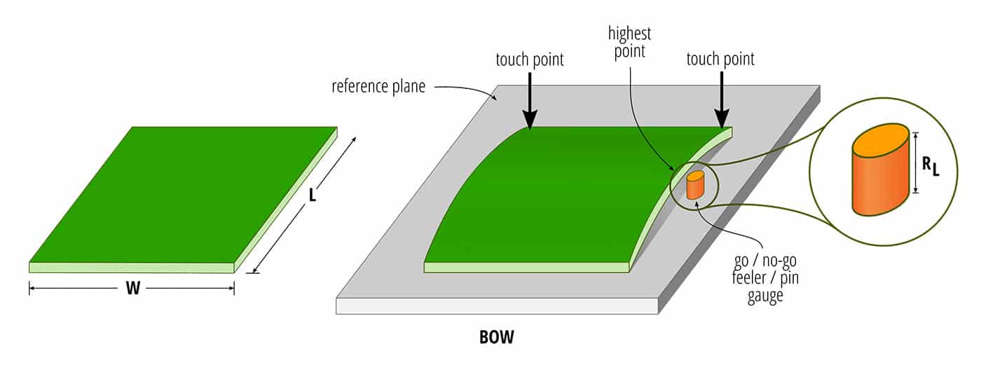
Measuring bow against a flat reference plane using a conceptual ‘go / no-go’ feeler / gauge / pin; the actual gauge is usually a piece of metal with precise, known, thickness. The process is repeated for the width with a feeler of RW thickness/height.
The procedure and calculations below are based on IPC-TM-650.
For measuring bow we first need to first calculate the maximum distance allowed for the length and width of the PCB we’ll be measuring:
Where RL and RW are the maximum bow distances for L and W, the length and width of the PCB, and B is the maximum allowable bow percentage. If, let’s say that our PCB is 200x300mm (L x W) in size and has SMD components (B=0.75%) we’ll have:
In which case the maximum distance from the bow’s worst point to the reference plane the PCB is measured should be less than 1.5 or 2.25mm along the length and width edges, respectively. If we then want to get the percentage of a bow we measured we can rearrange the formula. Let’s assume the bow distance we measured for the length was 1.4mm, so we have:
Measuring bow against a flat reference plane using a conceptual ‘go / no-go’ feeler / gauge / pin; the actual gauge is usually a piece of metal with precise, known, thickness.
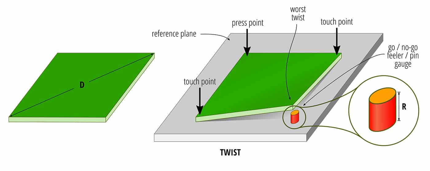
Measuring the maximum twist distance is similar but in this case we use the diagonal length:
Where D is the diagonal of the PCB and T is the maximum allowable twist percentage. The factor of 2 doubles the allowable distance because we are constraining one of the corners.
So, for the same parameters we used to calculate bow we then have:
To get the percentage from a measurement, we do the following:
For this method to be accurate, three of the four corners of the board must touch the reference plane with only one of them physically pressed. If this cannot be achieved, IPC-TM-650 describes a more complex ‘referee method’ that can be used.
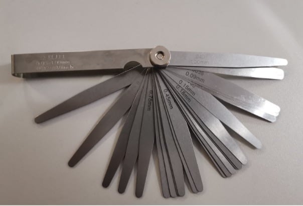
Thickness measuring tool set; these are the actual ‘go/no-go feeler/gauge pin’.
Warping happens due to an imbalance or asymmetry of materials when the stack is heated up and cooled down (during the process of pressing, etching, plating, etching, soldermask application, etc.). There are two primary causes for this kind of imbalance. Firstly, if the copper distribution across the board isn’t well distributed, and secondly, when PCB layers are not symmetric — in number and in thickness — above and below the horizontal centre of the board. In both of those cases materials shrink and expand at different rates, causing warps like bows and twists.
To avoid these issues, distribute copper as evenly as possible on all layers. When in doubt, it’s always a good idea to consult your PCB whether that distribution is good for robust production. And, unless it’s crucial for the application, always have a symmetric stackup of layers both in numbers and in thicknesses (except for single-layer boards of course).
Finally, the materials and process that the manufacturer uses are also crucial for minimising warping. They should use materials that are suitable for the manufacturing process; for every build use materials only from a single source; use horizontal ovens; and, let the boards cool down on a horizontal surface. Manufacturers should also be able to correctly ‘straighten’ boards when needed (by slowly heating and cooling the PCBs under weight). During assembly, PCBs should be dry and thermal shocks must be avoided by using suitable soldering profiles.
Measuring ‘bow’ on a PCB.
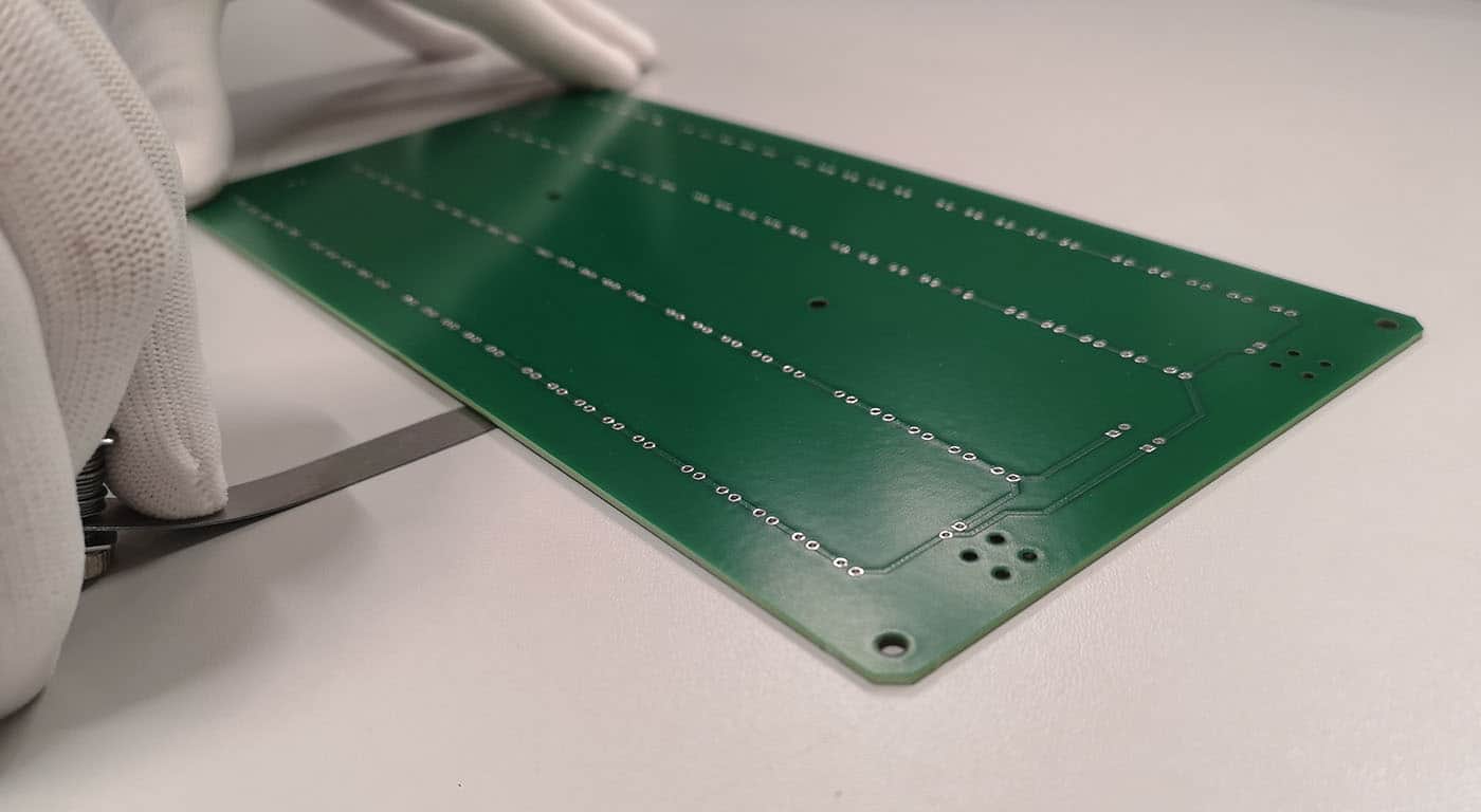
or measuring bows and twists we follow the methods as described above and adhere to the acceptable tolerances as defined in the IPC-TM-650 document.
All the stackups that we offer are symmetrical in all aspects in reference to the horizontal centre (except for the inherently asymmetric single-layer stacks). The plating simulator tool that’s available in our PCB Visualizer can show the copper distribution of your PCB. This information allows the designer to balance the copper distribution that may help reduce potential bow and twist. Finally, we have developed our manufacturing processes and procedures to minimise bows and twists as much as possible.