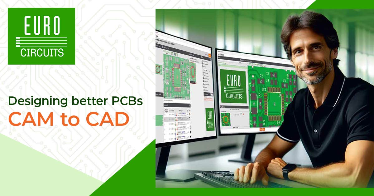
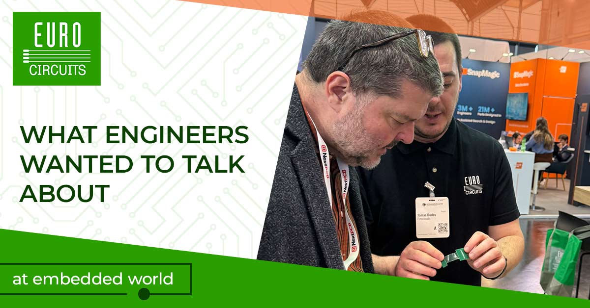
Eurocircuits Printed circuits blog

What keeps us busy at Eurocircuits, projects we are working at, new idea's, background information and a platform where you can participate, give your opinion and guide us to what is important for you as an electronics developer

Subscribe to feed Latest Entries

Eyes on the future, feet on the ground - Technology seminar by ACB

Posted by Marianne De Wolf
Marianne De Wolf
Marianne is the pcb technology expert within our Eurocircuits commercial team in
User is currently offline
on Friday, 04 May 2012
in Technology

On April 25, ACB organized their technology seminar….Eyes on the future, feet on the ground…

ACB, known in Europe as leading manufacturer of High Technology & Quick Turnaround Printed Circuit Boards, organized its first technology seminar.

The brand new CEO, Gilles Rigon, opened he seminar with explaining all about the ACB philosophy.   “S” for simple and easy solutions where possible, “S” for souple and flexible processes and “S” for Solid and reliable processes and how they balance their “eyes on the future” with their “feet on the ground” approach.  In fact, the importance of this balance would return in many lectures coming.

National Electronics Week a success.

Posted by Patrick Martin
Patrick Martin
Patrick is responsible for Eurocircuits sales in the UK and Ireland (and some ot
User is currently offline
on Thursday, 03 May 2012
in Meet Eurocircuits

National Electronics Week 2012 took place at the NEC in Birmingham on 18 – 19 April.  OK, it’s not really a week, but the organisers took over the name five or six years ago from a show almost lost in the mists of time.

Demand for prototype and small batch PCBs is strong.  A lot of people came onto the stand asking specifically how we could offer them a better prototype and small batch service. We explained our pooling services and demonstrated how to get prices off the website.  The response to the website and to the prices was very positive and we received our first order from a new customer two days after the end of the show.

We met a number of customers as well, always a pleasure.  Several had come specially to see the beta version of the new PCB Visualizer software which had its first public viewing at the show.  The new software will allow you to see your board layers as soon as the job is uploaded, so that you can check right away that everything looks OK.  PCB Visualizer will be rolled out over the next few weeks and more functionality will be added during the rest of the year to make handling data issues clearer and quicker.

On a lighter note our stand was a few metres from the “Bobs Box AKA the Cyclone Game Cube” as-seen-on-TV challenge.  Competitors stand in a transparent box and try to catch as many red balls as they can out of a shower of balls of many colours being blasted up from the floor.  Google it for YouTube videos.  This proved a big crowd-puller, especially when one or two short-skirted stand hostesses were trying.  No pictures of them, I’m afraid, but you can see Uwe Doerr in action.

Tags: Exhibitions

Large boards and pooling

Posted by Dirk Stans
Dirk Stans
Managing partner marketing and sales of Eurocircuits
User is currently offline
on Thursday, 26 April 2012
in Technology

Large boards and pooling – new guidelines


Over the last 12 months we have received an increasing number of boards in our pooling services at the maximum size allowed 425 x 425 mm.  These are not genuine single circuits but panels made up of many smaller circuits.  To get around our specified maximum panel size 350 x 250 mm, the individual circuits on these oversize panels are not profiled out.  In that way the users can describe the panel as a single circuit, though we know, of course, that they will subsequently cut out the individual circuits.


This practice raises two serious issues.


Het Instrument 2012 - AMSTERDAM RAI - September 25-28, 2012

Posted by Dirk Stans
Dirk Stans
Managing partner marketing and sales of Eurocircuits
User is currently offline
on Friday, 23 March 2012
in Meet Eurocircuits

Registration is open now

From the 25th until the 28th of September of this year we will have the pleasure of meeting you at the exhibition centre, RAI Amsterdam in Holland, Hall 1 Booth B031, for “HET Instrument 2012”.

While registering for a free entry ticket, you may also choose to register for a free gadget that you can collect on the exhibition.

This years gadget is the “compass clock”. The gadget is designed by our customer “YMIF engineering”. The realization and sponsoring of the gadget is again a broad cooperation between FHI member companies of which Eurocircuits sponsors and produces the PCBs.


Tags: Exhibitions

Elsyca Intellitool Matrix plating project

Posted by Luc Smets
Luc Smets
Managing partner Eurocircuits
User is currently offline
on Wednesday, 04 January 2012
in Technology

Eurocircuits'role in the project sets a new competitive standard

Making efficient pooling panels belongs to the core business of Eurocircuits. It is a necessity to ensure cost-effective production of prototypes or small batches. 
Eurocircuits started as a trader of printed circuit boards in 1991. Soon after, in 1993 we got involved in production. It has been our aim from the start to use pooling techniques for a number of reasons :

  • Save cost by increasing production efficiency
  • Save the environment by reducing waste

The idea of making pooling panels was not new in 1993. On the Benelux market a dutch company was already successfully offering single sided boards in pooling since the eighties of the last century. For double sided boards however it was not that common yet.

When we introduced combination panels for double sided boards in our own production in Hungary there was a lot of resistance from the operators and from the production management. They saw the complexity of their job increase, and technological challenges had to be taken care of.

Now, almost 20 years later, most technology issues have been taken care of, except for one major area, the galvanic copper plating.

For this galvanic process, the design of the PCB plays a vital role in the outcome of the process. In pooling panels there is even an influence of the design of one board on the copper deposition on surrounding designs. That means that we have to be very careful how to build our panel layouts.

The restrictions in panel configuration create limitations that affect the efficiency in our production. As a producer you can look at this problem in two ways:

  • Focus on efficiency and accept uneven copper distribution. Also accept that the quality of the PCB's produced for one customer can be influenced by the design of another pcb on the same pooling panel.
  • Focus on quality - stick to an even distribution and minimum copper plating thickness all over the panel. Accept that part of the panel surface gets lost because of extra copper areas and spacing introduced to balance out the galvanic layer. Also accept that not all jobs can be pooled with acceptable plating results.

Eurocircuits decided not to take any plating quality risks. We accepted the restrictions dictated by the plating process for a long time.The Elsyca Intellitool matrix copper plating is going to remove these restrictions.


Bow and Twist in printed circuits

Posted by Lengyel Norbert
Lengyel Norbert
Norbert is quality manager in Eurocircuits Kft
User is currently offline
on Tuesday, 31 January 2012
in Technology

What is Bow and Twist?

According to the IPC-A-600 standard bow and twist (flatness of the board) is :

“Flatness of printed boards is determined by two characteristics of the product; these are known as bow and twist. The bow condition is characterized by a roughly cylindrical or spherical curvature of the board while its four corners are in the same plane. Twist is the board deformation parallel to the diagonal of the board such that one corner is not in the same plane to the other three. Circular or elliptical boards must be evaluated at the highest point of vertical displacement. Bow and twist may be influenced by the board design as different circuit configurations or layer construction of multilayer printed boards can result in different stress or stress relief conditions. Board thickness and material properties are other factors that influence the resulting board flatness.”

Why is the flatness of a printed circuit board important?

  • During the production of the board the flatness of the panels is important for handling and for positioning the panels on the machines
  • During the assembly process the flatness of the panels is important for correct solder paste deposition and component mounting
  • Flatness is an aspect of the visual quality appearance of the boards.

What are the acceptability criteria for bow and twist?

  • For all boards the bow and twist should be 1.5 % or less
  • For boards using SMD components ( the majority of the boards) the bow and twist shall be 0.75% or less.

How to measure the bow and twist?

The IPC-TM-650 test methods manual describes the method to calculate bow and twist percentages

What can the PCB designer do to avoid bow and twist?


Industrial engineer master class visits Eurocircuits Kft

Posted by Luc Smets
Luc Smets
Managing partner Eurocircuits
User is currently offline
on Friday, 06 April 2012
in Meet Eurocircuits

On March 29 we welcomed the students from the first master year Industrial Engineer from the HELMo ( Haute Ecole Libre Mosane de Gramme- Belgium).

The students came to visit the Eurocircuits production plant in Eger, Hungary

Eurocircuits Data preparation - Make production panels

Posted by Luc Samyn
Luc Samyn
Responsible for frontend engineering at Eurocircuits
User is currently offline
on Wednesday, 11 April 2012
in PCB Design

By now your job has already been through two of the three front-end data preparation stages :

Stage 3 - Make production panels and production tools

We now have a stack of orders that are ready to go into production.

Our business model is based on “order pooling”.  We make our production more efficient by processing several different orders on the same production panel.  More efficient production means lower prices for our customers, especially for prototype and small batch orders. Which orders can be pooled together? This depends on a lot of factors, and finding the right balance is our daily challenge.

We need to consider:

  • Delivery term : we separate rush orders from standard delivery orders.  If we put both on the same production panel we could find that all panels have rush orders on them.  If every job becomes urgent, production efficiency goes down and our delivery performance is affected.
  • Order size : we keep large and small orders apart.  The higher the number of panels in a job, the longer it takes to process.  Production planning becomes less flexible and again we risk deliveries.
  • Copper distribution : we discussed this already in our earlier blogs about our new plating simulation tool and the Elsyca Intellitool Matrix plating project. We need to be sure that the designs we pool together don’t reduce each other’s plating quality.
  • Classification/complexity of the boards :  combining complex jobs with simpler jobs means that the final panel is more complex than it need be and so more expensive to produce.  That’s why we have two different pooling services ‘STANDARD pool' for standard boards and  'TECH pool' for more complex boards.
  • Technology: some technology options clearly can’t be combined with each other, for example different materials, copper weights and build-ups.  In other cases combinations might reduce production efficiency or quality. For example we could in theory combine boards with different legend colors on a single production panel.  In practice this would need two printing processes and two curing stages.  We would lose time at the print stage and risk the quality if the panel went through too many heating/cooling cycles.

The final decision day by day on which orders are combined on which panel is made by highly skilled and experienced engineers.  They have a growing number of software tools to help them to make the best decisions, and we are investing a lot of manpower and resources to develop even more powerful tools for the future.

Once the engineer has chosen the orders for the panel, how do we make it ready for production?

Eurocircuits data preparation - Analysis

Posted by Luc Samyn
Luc Samyn
Responsible for frontend engineering at Eurocircuits
User is currently offline
on Friday, 17 February 2012
in PCB Design

Have you ever wondered what we are doing to your data when the order status is Analysis or Single image? Here is the answer based on the instructions we give to our data preparation engineers. Many of the steps described below are automated for speed and accuracy but we have ignored this to make a clearer presentation. More information on our requirements can be found on the home page under “Technology Guidelines”.

Stage 1 - Analysis of PCB CAD data (Analysis and Analysis Cross Check)

Analyse the data files

  • Sort the data into Gerber files, Excellon drill files and any additional files (doc, txt, pdf, …) If the data comes in CAD format (EAGLE) convert into Gerber files, drill files etc.
  • Check the additional files: is there any job information there that is not in the Gerber/Excellon files or in the order (e.g. copper weights, soldermask colours, panel setup, tolerances, layer build-up etc)?

Convert the data into the format used by our data preparation software (DPF)

  • Upload and convert the Gerber and drill data. Is there critical information in aperture-lists, tool-lists or other files?
  • Check for undefined apertures or drill-tools (hole sizes) or 0-size apertures or drills
0-size aperture in the left image, should have been aperture 0.8 as in the right image.

Build the basic job

Eurocircuits data preparation - Single Image (part II) - other layers and outputs

Posted by Luc Samyn
Luc Samyn
Responsible for frontend engineering at Eurocircuits
User is currently offline
on Thursday, 01 March 2012
in PCB Design

Have you ever wondered what we are doing to your data when the order status is Single Image? Here is the answer based on the instructions we give to our data preparation engineers. Many of the steps described below are automated for speed and accuracy but we have ignored this to make a clearer presentation. More information on our requirements can be found on the home page under “Technology Guidelines”.

Stage 2 - Single Image data preparation (Single Image and Single Image Cross Check)

We covered before :

  • Eurocircuits data preparation - Analysis : the initial stage, checking if the data are complete and no obvious problems are there to fulfill the order.
  • Eurocircuits data preparation - Single Image (part I) - drill data and copper layers. : Verify and clean up the drill data and the outer and inner-layers.

This current article, Eurocircuits data preparation - Single Image (part II) - other layers and outputs, is our third article in a series about frontend engineering and is about the preparation of Soldermask, Silk screen (legend), coding on PCB's, making customer panels, machine outputs: "drill layer, rout layer, V-cut layer", SMD paste layers and optional other layers.

Solder-mask preparation

  • Replace any painted pads and areas with proper flash pads and polygons as for copper layers
  • Check for missing soldermask pads on component holes or fiducials
  • Check and add soldermask clearance pads on all non-plated holes
  • Check and correct the cover between the edge of the soldermask and the adjacent copper tracks or planes (= Mask Overlap Clearance or MOC) depending on the specification of the pattern class
  • Check and correct the clearance between the copper pad and the edge of the soldermask (=Mask Annular Ring or MAR) depending on the specification of the pattern class
  • Check and correct the minimum width of the solder-mask bridge between adjacent soldermask pads (=Mask Segment or MSM) depending on the specification of the pattern class
  • Save job

Eurocircuits data preparation - Single Image (part I) - drill data and copper image

Posted by Luc Samyn
Luc Samyn
Responsible for frontend engineering at Eurocircuits
User is currently offline
on Thursday, 23 February 2012
in PCB Design

Have you ever wondered what we are doing to your data when the order status is Single Image? Here is the answer based on the instructions we give to our data preparation engineers. Many of the steps described below are automated for speed and accuracy but we have ignored this to make a clearer presentation. More information on our requirements can be found on the home page under “Technology Guidelines”.

Stage 2 - Single Image data preparation (Single Image and Single Image Cross Check)

The name “Single Image” may be slightly confusing as it includes both single circuits and customer panels or assembly arrays. We use it to mean what we will deliver to the customer (individual circuit or panelised array) in contrast to our pooled production panels.

Build the job

  • load the job data received from Stage 1 (Analysis of PCB CAD data)
  • remove everything outside the board outline.
  • build a job netlist from the drill and Gerber data. We will use this later to check that we have not made any mistakes during the data preparation. If you have supplied an IPC netlist from your CAD system we will check the job netlist against this at this stage and raise an exception if we find discrepancies.
  • save a copy of the layers as received as a reference for later checks.
  • load the correct build-up for the job using the material thickness/copper thickness etc specified in the order
  • save the job.

Prepare the drill layer(s)

  • calculate the Nominal Hole Size. Where our standard tolerances (+/- 0.1 mm) apply, the nominal hole size is the finished hole size specified in the data (e.g. 0.80 mm). Where the designer has specified his own tolerance (e.g. +0.1/-0.00) we will aim to produce a hole in the middle of this tolerance band (so the Nominal Hole Size will be 0.85 mm).
  • increase the Nominal Hole Size to the Production Hole Size to accommodate the plating on the hole walls, the mechanical tolerances of the drilling machines etc. This is to ensure that every finished hole size is within tolerance. The rules are:
    • plated holes with finished diameter of 0.45 mm or less (taken to be via holes): increase by 0.1 mm.
    • plated holes with finished diameter of 0.50 mm or more (taken to be component holes): increase by 0.15 mm.
    • non-plated holes: increase by 0.05 mm. This is due to the bounce-back of the laminate: the drilled hole is always slightly smaller than the drill diameter.
  • Sort and regroup all drills and slots in the correct functional drill layer.
    • Put all drill and slots – PTH and NPTH - to the first drill run
    • Move any NPTH drill, slot or inner cut-out that is or can be seen as part of the board profile to the profiling run.
    • Move all NPTH drills larger then 6.00mm to the profiling run.
    • Move all NPTH drills and slots that are in a copper area (pad or plane) to the second drill run or the profiling run as per production requirements.

There are 3 possible steps in the production flow where we can drill holes:

  • First Drill Run or plated drill layer:
    • This is one of the first steps in production. All holes drilled here will become plated (PTH)
    • unless the hole is being covered with dry film, this process is commonly known as “tenting”
    • or “tented NPTH hole”. Tented NPTH holes MUST have a copper clearance of 0.30mm and can
    • have a maximum size of 6.00mm.
  • Second Drill Run or non-plated drill layer:
    • Is performed after the electroless plating process (or blackhole process). All holes here are non-plated (NPTH)
  • Profiling run or rout layer:
    • Is the last step where the profiling of the board is done. These holes are also non-plated (NPTH)

Outer Layer preparation

  • Clean the data
    • Replace any painted pads and areas with proper flash pads and polygons. Painted features filled with small draws were common in old-fashioned standard Gerber data but are not needed with Extended Gerber where you can define any pad shape or filled area you require.

More PCB added value on Stand 131 at National Electronics Week 2012 18 – 19 April, NEC Hall 2, Birmingham

Posted by Patrick Martin
Patrick Martin
Patrick is responsible for Eurocircuits sales in the UK and Ireland (and some ot
User is currently offline
on Thursday, 12 April 2012
in Meet Eurocircuits

PCB Visualizer will preview at the show

  • PCB Visualizer is Eurocircuits' latest added-value PCB service. Upload your data for an order or just a quotation. In seconds the new software will display every layer of your PCB just as it will be produced.
  • Instantly check each layer to make sure that it is what you need. Check that all the data is present and that the stack-up is correct. No need for a Gerber viewer. PCB Visualizer confirms your CAD output in realistic colours with full pan and zoom functionality.
  • Of course, our engineers check your board data 100% before we put an order into production or give you a confirmed quote. But if a quick glance shows you something that needs changing, you can correct it and upload new data and minimise lost time.
  • The first version of PCB Visualizer will be live online shortly. There will be new functionality added over the next few months to make buying boards from Eurocircuits even easier and even faster..

What else is new for 2012.

  • Faster PCB pricing and ordering for the first-time user. Get immediate prices online for all our pooling services without registering as a user – and store your prices in a basket for later ordering. Or order at once – your order goes straight into production with no administration delay.
  • New Design For Manufacturability (DFM) tool. An even copper density ensures optimum plating quality. Our new plating simulation tool can help you to achieve this. Use our "Place Inquiry" option and our engineers will produce a full manufacturability report on your board including a copper density visualisation map. DFM analysis can cut board costs up to 20%.
  • New technical support resources. The "PCB Design Guidelines" document is downloaded more than 30,000 times a year. Now we have added moretechnical papers as well as technical blogs and videos to help you design more robust and lower cost PCBs.
  • New bench-top reflow soldering equipment. We will show the latest models of our eC-stencil-mate solder-paste printer and eC-reflow-mate reflow oven, upgraded after feedback from more than 200 users in first 9 months of sales.

What’s old on the stand?

  • Always a warm welcome from our PCB and reflow-soldering experts ready to show you all the new features and answer your questions.
  • Our well-established order pooling services keep your costs down without compromising quality or delivery. We offer the widest range of pooling options including aluminium-backed and fine-line PCBs.


See us on Stand 131 at National Electronics Week, Hall 2, NEC, Birmingham 18 – 19 April 2012.


Can't make the show? Visit our homepage to check out the new features or contact Patrick Martin on 07834 281514 or at This e-mail address is being protected from spambots. You need JavaScript enabled to view it .

Tags: Untagged

eC-workshop – reflow soldering SMD PCB prototypes

Posted by Dirk Stans
Dirk Stans
Managing partner marketing and sales of Eurocircuits
User is currently offline
on Tuesday, 06 March 2012
in PCB Assembly

eC-workshop - Belgium  March 22, 2012

Eurocircuits are organizing a workshop on using the eC-reflow-equipment for the reflow soldering of SMD PCB prototypes.

Already 160 Eurocircuits customers throughout Europe are using our eC-reflow-equipment, the eC-stencil-mate and the eC-reflow-mate. Let us convince you of the ease of use, the quality and the reliability of our equipment at a dedicated hands-on workshop on SMD reflow soldering using our equipment.

The workshop is free. It will take place at 10:30 on 22nd March, hosted by our reflow soldering partner "ARCOSS" at Looiend 60 - 2470 Retie -Belgium

Specialists from Eurocircuits and ARCOSS on the eC-reflow-equipment and SMD reflow soldering will be on hand to demonstrate the equipment and to answer all your questions on the reflow soldering of surface-mounted devices.

To register for this event or to request additional information complete this form.

Registration for the workshop will close on 15 March or earlier if the maximum number of attendees is reached before this date. In this case we will arrange a second workshop on a later date.

More detailed information on our eC-reflow -equipment can be viewed here.

Which surface finish fits your design

Posted by Marianne De Wolf
Marianne De Wolf
Marianne is the pcb technology expert within our Eurocircuits commercial team in
User is currently offline
on Friday, 09 March 2012
in Technology

Surface Finishes on printed circuit boards

Then finally, you have finished your design and the moment has come to order the PCB.  You have considered all the important aspects. The DRC check is done and you are relieved: no errors remaining.

The online calculator shows you the default pooling options and offers you the possibility to adjust some of them to your specific need.  En there you bump onto the Surface Finish.  What is Surface Finish and how to make the right choice?

Since all finishes have advantages and disadvantages, it is important to stand still by their application and to check how your boards will be treated during assembly.   The different finishes we offer are Lead-free HAL, Electroless Nickel/Immersion Gold (known as ENIG) and Immersion Silver (ImAg).  All of these are Lead-free and can be used for a RoHS design but also in a SnPb assembly.  Edge connectors can be covered with hard Gold (electroplated Ni/Au).

new CadSoft EAGLE DRU files for EAGLE V6

Posted by Luc Samyn
Luc Samyn
Responsible for frontend engineering at Eurocircuits
User is currently offline
on Monday, 09 January 2012
in PCB Design

New as from 21/02/2012:

Eurocircuits is appointed as value added reseller of Cadsoft EAGLE, so the EAGLE software is available from now on through our web-interface.

New in EAGLE Version 6

In the new EAGLE Version 6 format, the EAGLE brd-file is saved in XML format. Also new in EAGLE version 6 is that the used Design Rules Settings (used DRU-file) are embedded and saved in the EAGLE board file (EAGLE brd-file).

In the previously released EAGLE design rules of Eurocircuits (eC-EAGLE-design-rules-24-06-2011.zip) the DRU file description contained quote-characters (“), which are not supported as such in the XML format.

Using these “old” eC-EAGLE-design-rules in EAGLE Version 6 will lead to errors when trying to load a Version 6 EAGLE brd-file which has been saved with the “old” eC-EAGLE-design-rules. The eC-EAGLE-design-rules have been updated to correct this problem:

ec-eagle-design-rules-14-02-2012.zip

When you downloaded the eC-EAGLE design rules earlier and you did not upgrade to version 6 yet, you do not need to install these new DRU files. When you upgraded to version 6 of EAGLE we advise to use these new design rule files.

Design Rules


Southern Manufacturing and Electronics Show 2012 a success

Posted by Patrick Martin
Patrick Martin
Patrick is responsible for Eurocircuits sales in the UK and Ireland (and some ot
User is currently offline
on Wednesday, 29 February 2012
in Meet Eurocircuits

In February? In a tent? The SME show really shouldn’t work, but year after year, even through the snow, the visitors still arrive. This year there was no snow and a record attendance.


Dirk Stans, Uwe Doerr and myself were kept busy by visitors throughout. Uwe gave repeated demonstrations of the eC-stencil-mate solder-paste printer and the eC-reflow-mate reflow oven - and successfully. This was the first show ever where we sold both machines off the stand and they were on the users' premises within 3 days of the end of the show. There was plenty of active interest in our prototype and small batch pooling services. By the second day of the show we had received the first 2 day turnaround orders from a prospect we had met on day 1.

Missed us and want to know more about Eurocircuits and our products and services? Contact Patrick Martin on 07834 281514 or at This e-mail address is being protected from spambots. You need JavaScript enabled to view it .

Tags: Exhibitions

Eurocircuits integrates EAGLE CAD software

Posted by Dirk Stans
Dirk Stans
Managing partner marketing and sales of Eurocircuits
User is currently offline
on Sunday, 26 February 2012
in PCB Design

Eurocircuits integrates EAGLE CAD software

Eurocircuits have been appointed pan-European Value-Added Reseller for CadSoft’s EAGLE PCB design software.  Now you can buy EAGLE CAD software licences and upgrades directly from our website on your Eurocircuits account – no need to set up new accounts and payment procedures.  How?


Why do we offer a CAD package?

We want to offer our customers more than just a top quality prototype and small batch PCB service.  We want to help them speed up their development cycle and get their products to the market faster.  The key to this is integration.  We want to provide the tools for an integrated workflow from design to assembled product. Whether you are a prototype designer or a small batch manufacturer, an integrated workflow will deliver faster product development with less risk of error and lower costs.

Downstream we have integrated our PCB and stencil products with reflow soldering.  This is already showing benefits.  Customers report that using our bench-top stencil printer they can cut assembly time by up to 75%.  In particular the eC-registration system aligns the board and stencil fully automatically, cutting out the time-consuming manual alignment needed on traditional printers.  Our bench-top reflow oven completes the process.

A CAD package allows us to integrate upstream.

Why EAGLE?

Eurocircuits Then and Now

Posted by Sandip Parekh
Sandip Parekh
General Manager Intellial Solutions and project leader of the Eurocircuits softw
User is currently offline
on Thursday, 16 February 2012
in Eurocircuits strategy and history

The Eurocircuits website - Then and Now - From website to online ERP system

We have come a long way, the simple website we launched to let customers calculate and order the PCBs online has grown into a complete ERP system now. But the initial philosophy to create one unique platform where all information is available to both customers as internal staff remains the same even now. This post is an attempt to give you a glimpse of evolution of the website.

The Beginning (2000-2002) - version 1

Homepage - Year 2002


Tags: Software

Eurocircuits Sales figures 2011

Posted by Dirk Stans
Dirk Stans
Managing partner marketing and sales of Eurocircuits
User is currently offline
on Monday, 06 February 2012
in Eurocircuits strategy and history

Presentation of the sales results 2011

Sales

2011 was a good year. For the first time our PCB turnover exceeded 15M€. The total consolidated group turnover including equipment sales amounts to 16.9M€.

Overall sales increased 3.57% against  2010. Our online pooling services showed a healthy  growth in sales value of 14.14 %.

The turnover evolution in PCB sales over the last 5 years is as follows :

  • 2007 - 11.9 million  €
  • 2008 - 11.8 million  € 
  • 2009 - 11.8 million  €
  • 2010 - 14.8 million  €
  • 2011 - 15.4 million  €


Hand-soldering - point by point or mini-wave technique

Posted by Ben Verwaest
Ben Verwaest
Ben is director of Arcoss BVBA, an expert in repair, rework, training and consul
User is currently offline
on Monday, 13 February 2012
in PCB Assembly

Hand-soldering with the same high quality result as reflow or wave soldering?

Are you ready for the challenge ? Let us look at  the mini-wave soldering technique.

This picture shows that tools and skills are the basics to achieve a good result in hand-soldering. You agree ?

Hand-soldering is in most cases the last step in the prototype assembly process. Why is it less controlled and more difficult than other steps in the manufacturing. It is something we all know how to do. It's just heating up a PCB and a component to make a solder joint. Isn't that simple?

PCB designers, technicians, electronics engineers, we all learned at school how to solder with an iron. It can be 5 or 35 years ago, but we assume that not a lot has changed. A lot did change!

Do we still take our car to a service where they have only mechanical hand-tools to fix it ? They do have a lot of tools these days to do a good repair job.