Developing our HDI pool manufacturing process

Author: Saar Drimer /
Figure 1. A test panel.

We have recently introduced the HDI pool, enabling our customers to design and have us manufacture and assemble PCBs with BGAs down to 0.4mm pitch. Developing this service required testing to make sure our manufacturing process is robust for all types of designs that we may receive. Here we will discuss some of these tests, which, in addition to validating our process, yielded gorgeous images that can also teach us a lot about PCB manufacturing.

The Structure

Figure 2. The HDI 8-layer pool buildup.

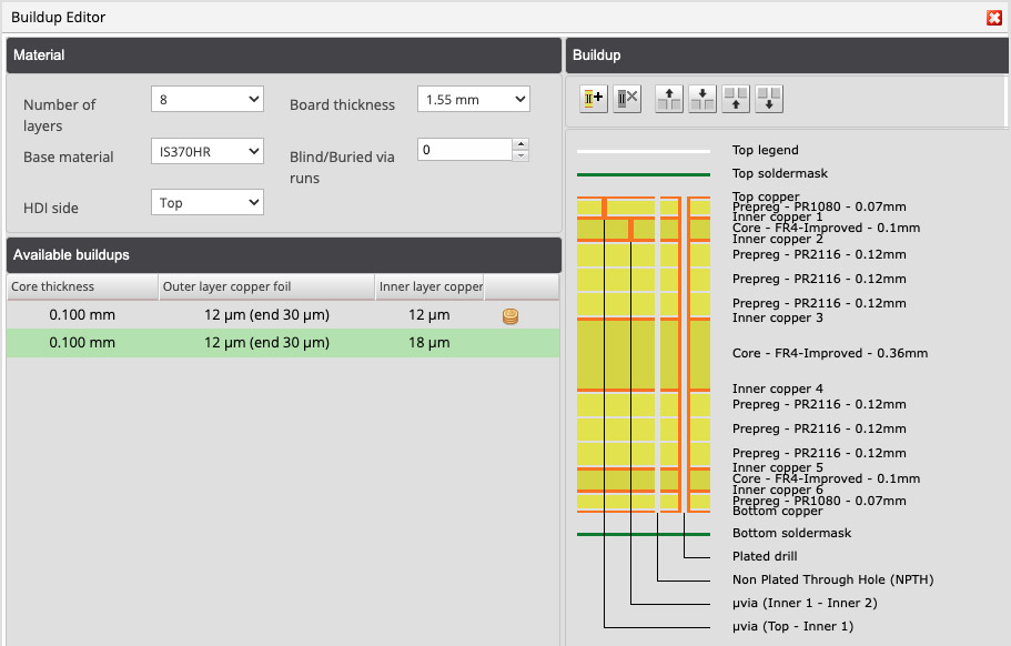
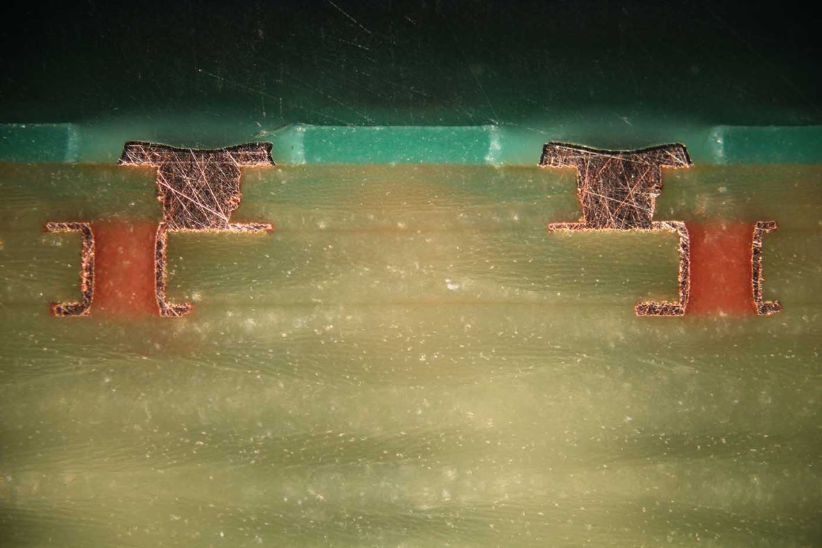
What we currently offer through the HDI pool are 0.1mm diameter microvias from layer L1 and L2, and from L2 and L3 (or, alternatively, L6-L7 and L7-L8) on an 8-layer buildup shown in Figure 2. This structure is beautifully shown in Figure 3: a cross section at the centre of two sets of staggered microvias. Looking at this image we’re able to notice the following details:

  • The L1-L2 substrate is slightly thinner than the L2-L3 substrate as seen in the Figure 2 buildup.
  • The L1-L2 microvias are created by laser, which is hinted at by the typical slight tape. We also see that these vias are filled with copper during the manufacturing process.
  • The L2-L3 microvias are mechanically drilled through the ‘core’ – thus, not tapered – and plated. During the pressing of the layers the solidified prepreg above and below this core fills the microvias.
  • The L1-L2 and L2-L3 microvias are staggered, not stacked; we require that holes are non-overlapping with a minimum of 10μm clearance.
Figure 3. The L1-L2 and L2-L3 microvias. The L1-L2 microvias are lasered and filled with copper whilst the L2-L3 microvias are drilled, plated and filled with hardened prepreg.

The Tests

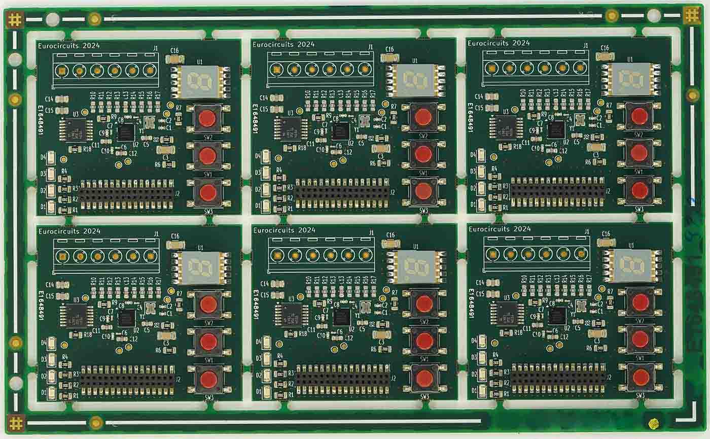
2nd The test panels have gone through a process similar to the one our customers’ panels will go through; the purpose is to test the correct application of solderpase, that there are no manufacturing defects, and to examine the effects of heat cycling. text relating to sub title above or just general newsletter text

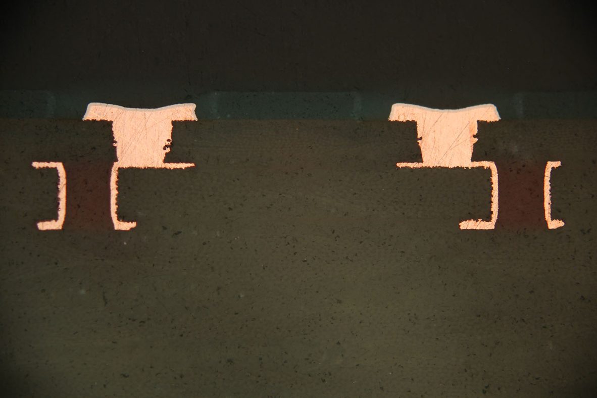
For better inspection of the microvias’ structure we can look at a higher contrast version of Figure 3, shown in Figure 4, where the intersection of the copper and the substrate is quite clear. We’re looking for gaps in the copper and where it may be thinner than a certain minimum. What’s also interesting to see here – something that is rarely seen by PCB designers – are the fibreglass strands’ ‘imprint’ on the plated copper; more on the finer details of FR4 is here.

Figure 4. Higher contrast version of Figure 2 where it’s easier to look for defects.

Next, let us look at the design itself, shown in Figure 5. We can see the 0.4mm pitch BGA in the centre with various other components around it; a more detailed view of the BGA is shown in Figure 6. Please refer back to these images whilst reading on.

Figure 5. A large portion of the PCB we tested (only the first three layers are shown). The white circles are the annular rings of 0.15mm hole through-vias.
Figure 6. A detailed view of the BGA. Notice the L1-L2 microvias in the centre of pads, and the L2-L3 microvias that are ‘staggered’ compared to the ones above them. (Only the first three layers are shown.)

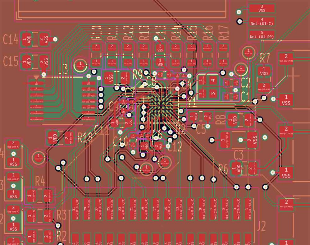
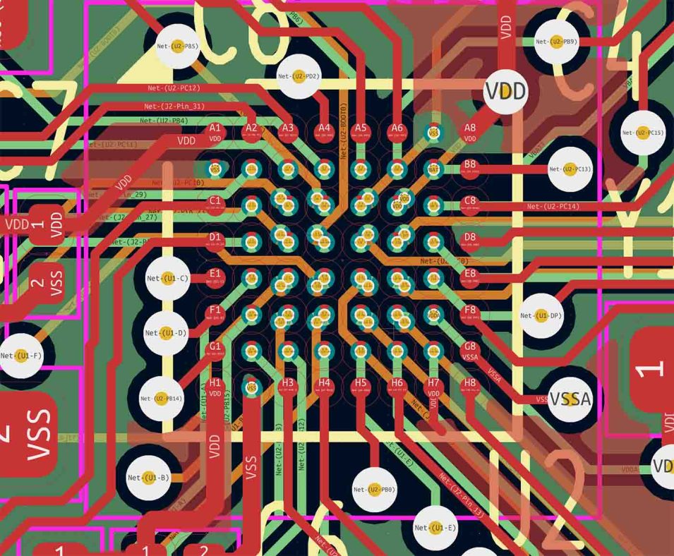
Figure 7 shows an x-ray of the board after applying solderpaste using a stencil. We’re able to examine the application of the paste to observe if there’s an offset or possibly excess paste, and that the paste was correctly applied through the tiny holes. (We also have our separate ‘solderpaste inspection’ tools, SPI, for such tests.) The interesting details to note in this image, that are not visible later when the BGA is soldered, are the microvias below the BGA pads and how much smaller they are compared to ‘regular’ through-vias (the four large columns in the centre).

Figure 7. The board after the application of solderpaste. Notice the tiny microvias below the pads and how much larger the ‘regular’ vias are.

Reflowing – heating and cooling cycles at temperatures used for component assembly – causes air, liquids, and trapped impurities within the copper and isolation substrate to expand; this view makes defects much easier to notice since the defects breach the surfaces. For this test we have reflowed the board four times with some components placed. Figure 8 shows a top-view x-ray of the board after reflow (compare it to figure 5).

Figure 8. An x-ray of the manufactured board after reflow and some components assembled. The BGA component is there, but is nearly invisible. Also notice the inner routing of the 7-segment display chip to the left of the BGA.

Next we have a closer look at the BGA at an angle that allows us to observe more detail; this is shown in Figure 9. We are mainly looking for the following:

  • Shorts between the pads which will indicate that there was too much paste applied. This could happen if there’s a tiny gap between the stencil and the board so paste had creeped underneath the opening, or that the stencil wasn’t sufficiently clean.
  • Misalignment of the BGA. Beyond a certain misalignment threshold, the solder doesn’t ‘shove’ the component into place, and that would be visible here.
  • Missing or imperfect solder joints, which will show as two solder blobs on the same pad instead of a perfect ball, like in Figure 9.
  • Imperfections in the copper such as voids that happened during reflow.
Figure 9. An x-ray after soldering the BGA. The solder balls are larger than those in Figure 7, and show none of the faults we’re looking for such as shorts, misalignment, or bad solder joints.

Conclusion

Developing a new manufacturing product takes a lot of testing to make sure that the production process is robust, particularly so when it comes to miniaturisation. Developing the HDI pool required all of our prior manufacturing expertise, and new machines, in order to provide a cost effective solution for our clients’ need to design with high-pitch BGA. Give it a try!


Bring your product to market on time and within budget – join the Eurocircuits Community

LinkedIn icon Facebook icon X logo in Eurocircuits Green You Tube icon eC TV logo in black

Bring your product to market on time and within budget – join the Eurocircuits Community