DFM – From Gerber files to PCB production data
The board designer has prepared his layout on a Computer Aided Design or CAD system. Each CAD system uses its own internal data format, so the PCB industry has developed a standard output format to transfer the layout data to the manufacturer. This is Gerber. The Gerber files define the copper tracking layers (4 in the job we are following) as well as the soldermasks and component notations.
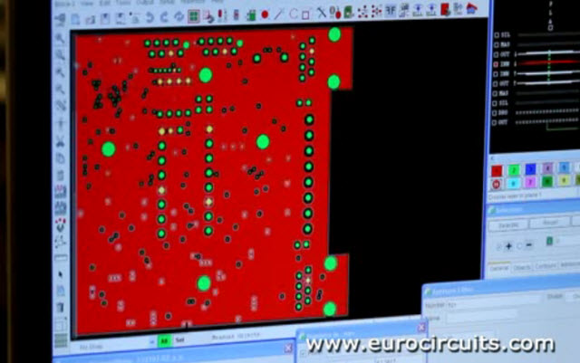
First we check that data meets our manufacturing requirements. These checks are mostly done automatically. We check the track widths, the space between tracks, the pads around the holes, the smallest hole size etc. The engineer can also check and measure individual areas where he wishes. Once the data is verified as good he will output all the tool files needed to drive the machines that will make and test the PCB.
More information about the front-end data preparation process
Return to the process overview – Making a PCB – PCB Manufacture step by step