Copper and the Board Edge
Copper and the Board Edge
There are three options under our Advanced options heading which may be confusing:
- Copper up to board edge
- PTH on the board edge
- Round-edge plating.
Here’s how to sort them out.
Copper up to Board Edge
To avoid damage to the copper during the profiling operation we normally ask for a minimum distance between the copper features and the edge of the PCB. This distance is:
- 0.25 mm on outer layers with breakrouting
- 0.40 mm on inner layers with breakrouting
- 0.45 mm on all layers with V-cut scoring.
These figures are needed to accommodate industry-standard manufacturing and machining tolerances. For V-cut scoring it is also necessary to accommodate the V of the cutter.
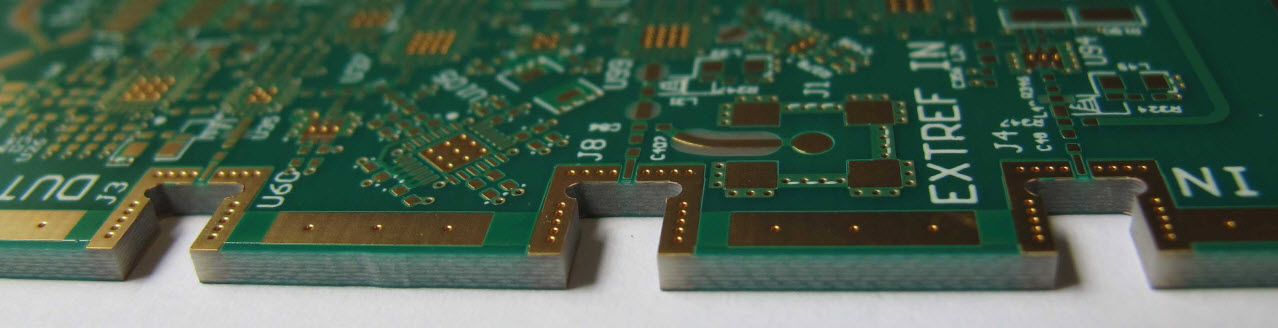
Sometimes it is necessary to run a copper plane up to the board edge. In this case select “Copper to board edge”. There is no extra charge for this but it alerts our engineers to set up a different cutter speed.
“Copper to board edge” should normally only be used for planes and large copper areas where any slight damage to the copper will not impact on the performance of the PCB.
Tracks must not be placed within the minimum distance of the board edge where they could be damaged. Our engineers will raise an exception whenever they find tracks within the exclusion zone.
If we find pads within the minimum distance of the board edge, we will clip them back to restore the minimum copper-free space unless:
- the pads are part of an edge connector (usually with a bevelled edge)
- the pads are marked as “up to the board edge” in a separate mechanical layer
- the clipping is more than 25% of the pad surface in which case we will send an exception to the customer.
Note
Copper to board edge cannot be combined with V-cut scoring.
Tip
We will always cut inner layer planes back by 0.40 mm to avoid any risk of shorting.
PTH on Board Edge
Also called “castellated holes”.
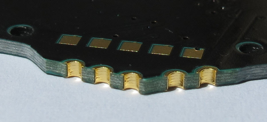
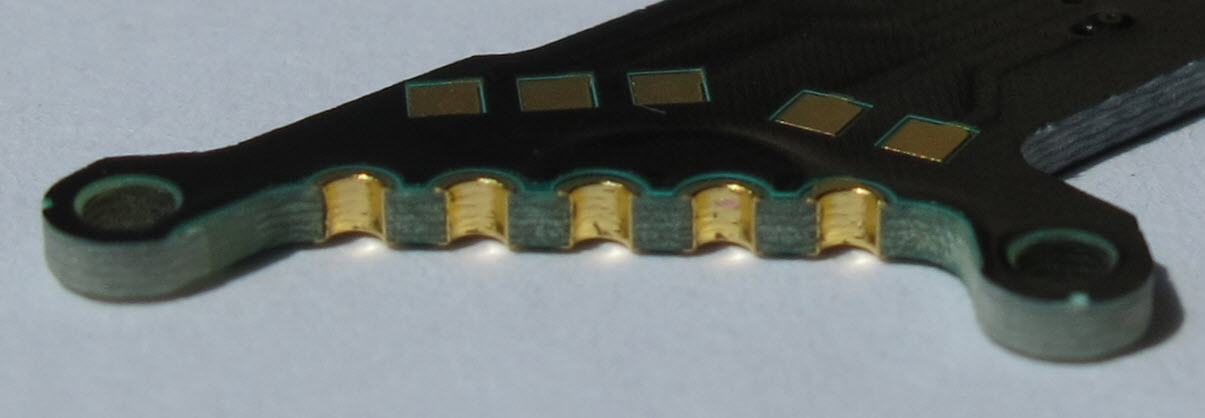
These are plated holes cut through on the board edge and used to join two PCBs either by direct soldering or via a connector. As the process requires extra steps, plated holes on the board edge are a cost-option.
Your data should clearly show the holes and the profile. Ideally include the information in a mechanical layer.
Tips
- There must be enough spare space on the edge of the PCB for us to hold the PCB in the production panel during manufacture. If you need castellated holes on all 4 sides, email us your design or proposed profile as early in the design process as possible. We can then confirm that it is manufacturable or suggest any necessary changes.
- You must have pads on top and bottom layer (and on inner layers where possible) to anchor the plating securely to the PCB.
- As a general rule the holes should be as large as possible to ensure good soldering to the mother PCB. We recommends 0.80 mm and above.
- All surface finishes are possible but our preference is for selective gold over nickel for the smaller sizes.
Round Edge Plating
This means that most or part of the edge of a PCB or a cut-out is plated from the top side to the bottom side.

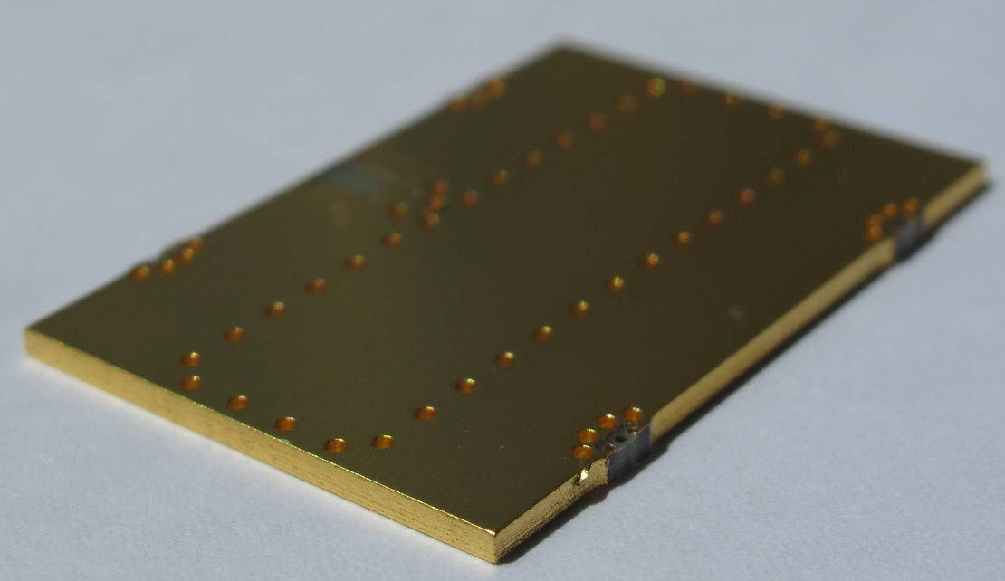
This may be to ensure a good ground to a metal casing or for shielding purposes.
To manufacture a board with round-edge plating we rout the board profile where the edge plating is required before the through-hole plating process. This involves extra process steps so round-edge plating is a cost option.
Tips
- There needs to be a band of copper on each side for the plating to connect to.
- As we need to hold the circuit within the production panel during processing we cannot plate round 100% of the edge. There must be some gaps so that we can place rout tabs. If you need a very high percentage of edge-plating, email us your design or proposed profile as early in the design process as possible. We can then confirm that it is manufacturable or suggest any necessary changes.
- Indicate clearly in a mechanical layer where you need round-edge plating.
- Selective chemical nickel-gold is the only surface finish suitable for round-edge plating.