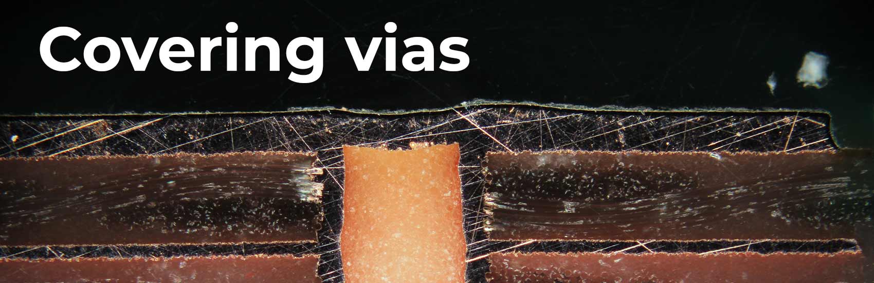
Covering vias
Vias are plated holes that connect signals between layers, and are typically smaller than ordinary plated holes that are used for soldering through-hole components. What also makes them special is that they’re usually not the destination of a signal, so they create a physical ‘interruption’ that sometimes makes an impact on functionality.
Types of vias
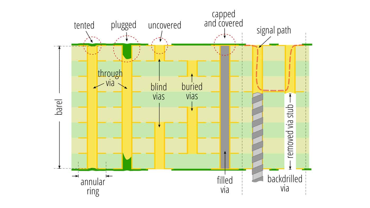
A typical via is made of an annular ring at the PCB’s component layers, and some internal layers, with a conductive barrel connecting all of them. There are three primary types of vias:
- Through: spans the entire stack of the board.
- Blind: starts on a surface layer and ends in an internal layer.
- Buried: starts and ends in an internal layer.
Then we have vias that are
- Tented: via surface covered with dry film soldermask.
- Plugged: openings at surface layers are stuffed with liquid soldermask.
- Filled: entire barrel is filled with conductive (copper) or non-conductive (resin) materials.
- Back-drilled or Controlled Depth Drilling (CDD): via is partially drilled through the board to remove an ‘unused’ stub that can cause an impedance mismatch on defined impedance boards.
(There are also microvias ― 1:1 diameter-to-depth ratio and not exceeding 0.25mm in depth ― that are sometimes created with a laser. Microvias can be stacked or staggered and are used with High Density Interconnect (HDI) boards. More about microvias is outside the scope of this article.)
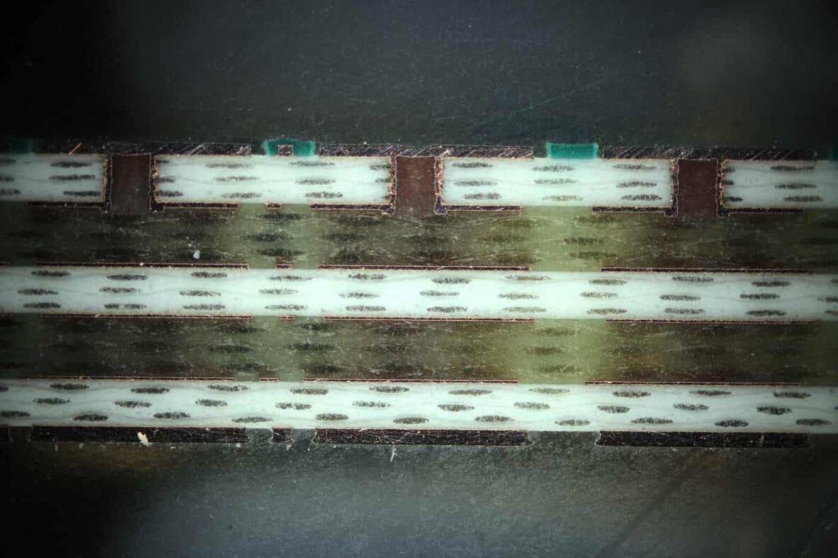
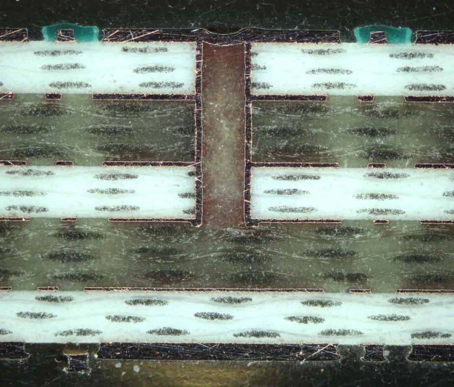
Most PCBs are made by pressing a stack of a combination of copper foils and dielectric materials (FR-4, RO4350, IS400, as cores or prepreg sheets). The combinations and ratios of these is how different thicknesses and multi-layer PCBs are created. Through-vias are drilled after pressing the entire stack together while blind- and buried-vias require drilling only some of the stack’s layers before the complete stack is pressed together.
Tenting, plugging, filling, capping, and covering

A via leaves a hole exposed on the surface of the board and we’d sometimes like to protect it. For example, we may want to
- cover the hole so that the signal isn’t exposed;
- place a pad on top of a via (via-in-pad );
- prevent flux, solderpaste, covering materials, and adhesives from flowing through the hole, cause faults and defects; or
- make the board look better by being able to completely cover the via with silkscreen.
There are three techniques for protecting vias: tenting, plugging, and filling, as I defined earlier.
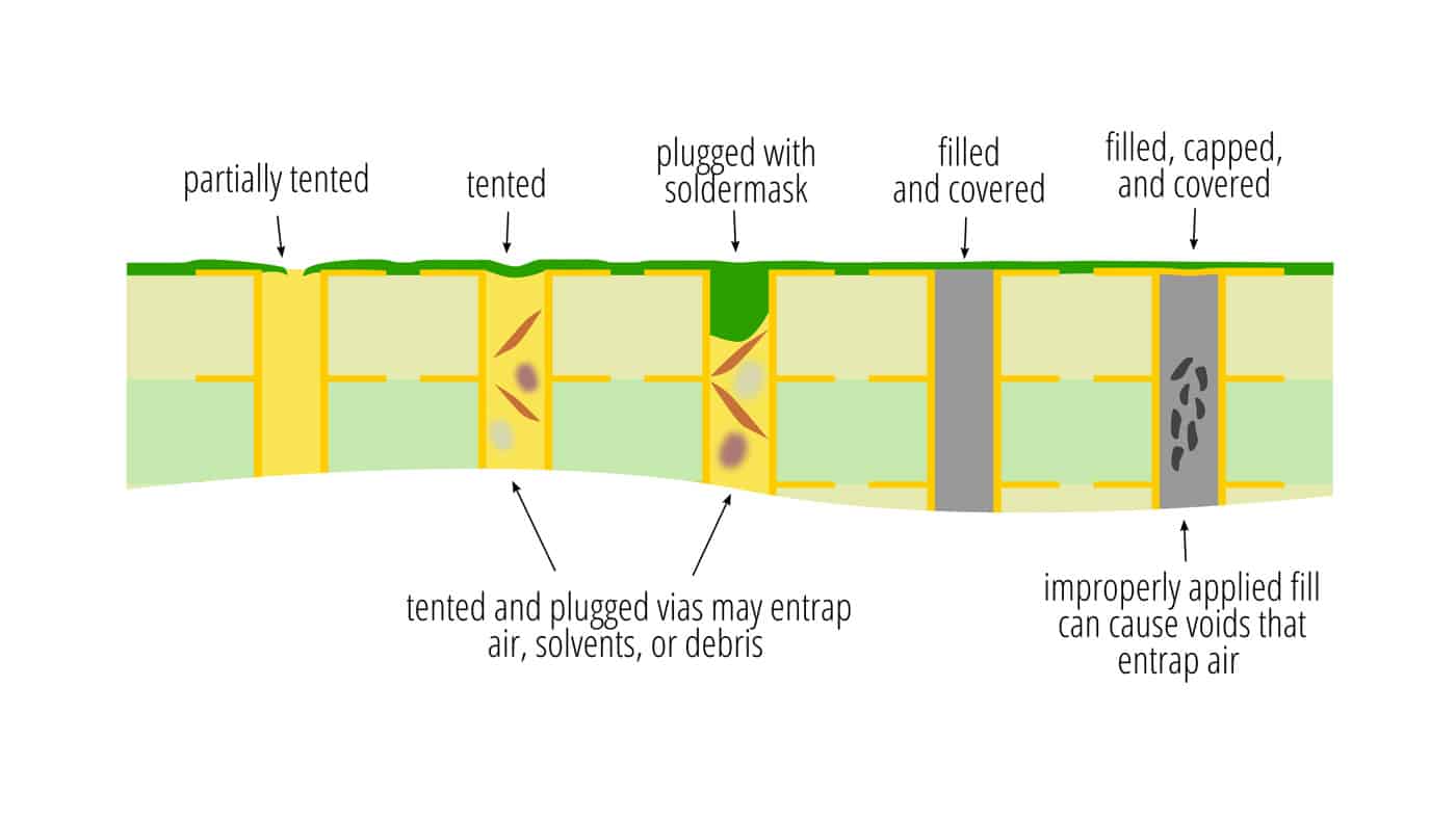
Via tenting is done using dry film soldermask to cover the hole (either in a single process with the rest of the board or as by applying cover dots before another soldermask pass). Via plugging is achieved by pressing liquid soldermask into the vias using a squeegee and then applying soldermask (dry film or liquid) to the rest of the board.
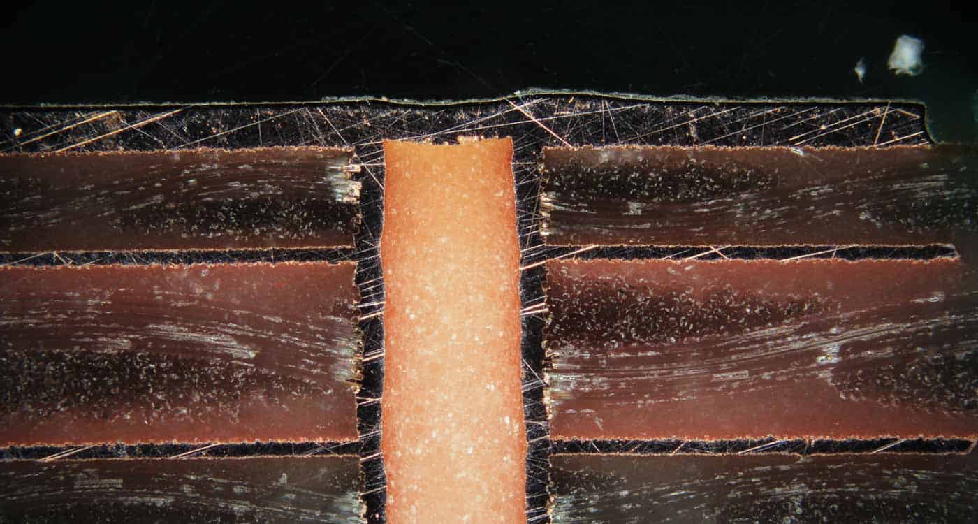
Whether the via’s hole is reliably tented or plugged, though, depends on the size of the barrel, the thickness and viscosity of the soldermask, how soldermask is applied, and the effectiveness of the curing process. Therefore, across the many variables there is no guarantee that a hole will be appropriately covered. Crucially, tenting and plugging vias may entrap air, debris, solvents, contaminants, and other materials from the manufacturing process that cannot be removed in subsequent cleanup stages. Entrapped elements can cause eventual defects in the barrel, but also blow-outs when the trapped gasses expand during curing and soldering. These blow-outs can result in soldermask teardown, exposing the copper to oxidation and contamination, which may lead to defects in the short- and long-term. In fact, some companies forbid tented and plugged vias altogether for this reason.
It’s sometimes helpful to place a via just a pad ― this is called via-in-pad ― or very close to one where there cannot be any soldermask in between the pad and the via. This may be good for signal integrity, tricky signal fanout, or tight routing spots. If we do that without consideration, though, the via opening creates a nonuniform pad surface and can wick the solderpaste that’s used for soldering components; both of these things cause bad solder joints. Designers, therefore, choose via filling where the via is filled and only then a uniform pad is manufactured on top of it. Filled vias can be capped with copper and covered with soldermask.
Filling vias requires additional steps to the ordinary PCB manufacturing process: drill the vias that need filling; clean (plasma and brushing); apply conductive carbon; apply dry resist film/mask; imaging of only the holes that are to be filled; apply copper through galvanisation; strip resist; brush/deburr/clean; bake for one hour; fill holes with resin; bake for one and a half hours; brush/deburr/clean. Then the panel can go through the rest of the steps that all PCBs go through (drilling, plating, imaging, and so on).
What about blind- and buried-vias? Buried vias ― those with no exposure to the surface ― are inherently “filled” through the process of stacking of the layers where the prepreg sheets become malleable and flow into the barrel. This also happens on the internal side of blind vias but the extent of the “fill” towards the surface is indeterminate, so the considerations discussed earlier still apply.
Finally, in transmission lines carrying high-frequency signals, stubs cause impedance-mismatches that distort the waveform by causing reflections. Back drilling, or Controlled Depth Drilling (CDD) is a technique that drills out the stubs which are the bit of the via that isn’t required for carrying the signal.
Vias at Eurocircuits
Eurocircuits offers through-, blind- and buried-vias. We use liquid soldermask that is superior in its adhesion and solderability and that enables better results during optical inspection and component alignment for assembly. Liquid soldermask is spray-coated onto the board (so it is unsuitable for via tenting) and is compatible with our advanced direct imaging system that allows much tighter registration accuracy. For all those reasons and the inherent unreliability of via tenting and plugging that we discussed above we do not offer these types of via protection. (For completeness, at the time of writing our liquid white and transparent soldermasks are applied using film exposure not through direct imaging.)
Instead of via tenting and plugging we offer the much more robust resin-filling of vias that’s always capped with copper (we’re only able to fill through-vias). The designer can then decide to place a pad on the area above the via, leave it uncovered, or cover it with soldermask. Follow our guide to see how to tell us that you’d like filled vias and to which vias to apply it to.
In order to define that you require blind- or buried-vias and what layer span they occupy use our Buildup tool; the user guide for this tool is here.
Bring your product to market on time and within budget – join the Eurocircuits Community


![]()

