Let’s talk about Outlines
Hello! This is the first article in a series of six where I cover PCB design and manufacturing topics: outlines, courtyards, annular rings, keepouts, fiducials, and copper fills. We will publish the series weekly as part of our ongoing Technology Thursday publications. To make sure that you don’t miss them please follow us on the various social platforms or join our mailing list. Now let’s talk about outlines!
An outline, sometimes also called a contour or profile, defines the physical border of our circuit-board and can be a simple rectangle or an elaborate shape. Outlines may seem like a trivial thing to define, but the reality of manufacturing actually makes it a complex issue with many potential pitfalls. Here I will describe these issues in order to help you avoid them at design time rather than at 2am when submitting the board, or worse, when you get it back!
Defining the outline
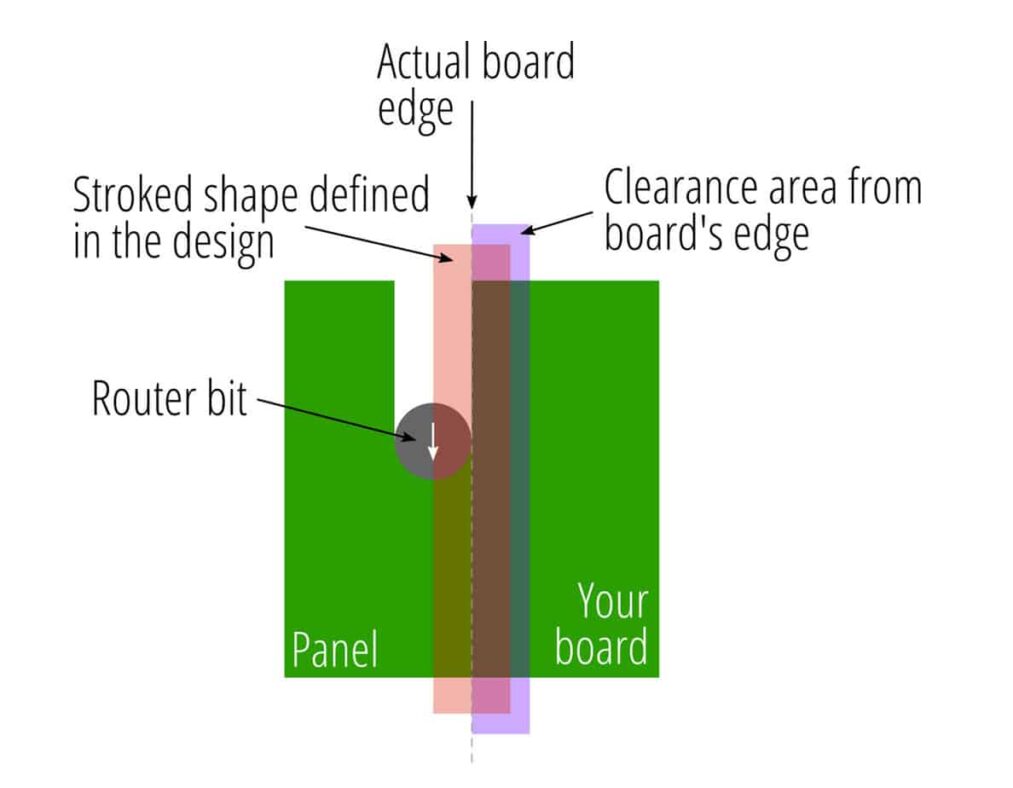
We define an outline in a dedicated ‘layer’ of our EDA tool. The shape is meant to be defined by a closed and non-intersecting line that’s normally displayed stroked with a certain width, but unfilled. By convention it’s the middle of that stroke width that’s taken as the actual board outline. Seems simple, but here’s what could go wrong:
- The stroke width is purely there to help us see the shape. Its middle isn’t normally displayed to us, so accurately aligning other features close to the outline can be haphazard. Because of this I’d recommend the thinnest stroke width that you can handle or one that provides additional information. (For example, 0.5mm stroke allows you to ‘see’ a 0.25mm clearance from the edge; 0.8mm the UL clearance of 0.4mm; and, 0.9mm clearance of 0.45mm for V-cut boards.) It’s also a good idea to use your tool’s grid, alignment, and snapping abilities to make sure features are accurately placed.
- Due to confusion over origins some EDA tools don’t align the outline correctly with the rest of the features of the board when exporting manufacturing data. This means that the exact placement is ambiguous to the manufacturer, and they may or may not fix it correctly or even ask for you to confirm the changes. To help I’d recommend viewing the output files with Gerber viewers that are ‘external’ to your normal process, like the free Gerber viewer from Ucamco, the maintainer of the Gerber format. And, if the fab allows it, reviewing the post-processed design files before approving the design for production.
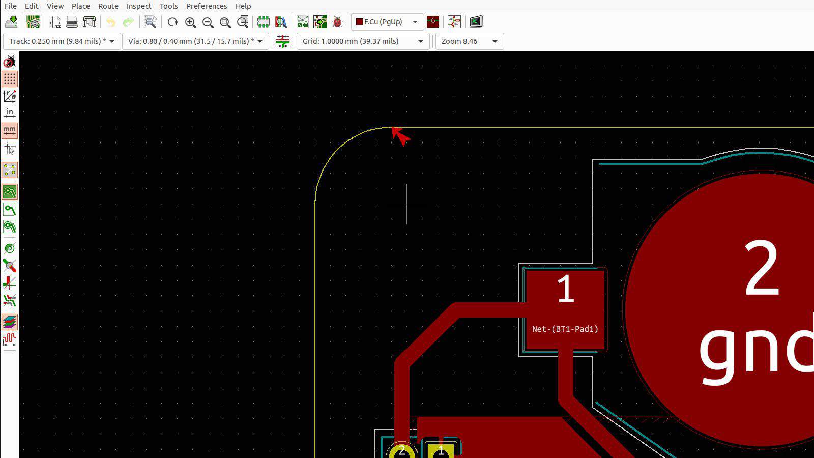
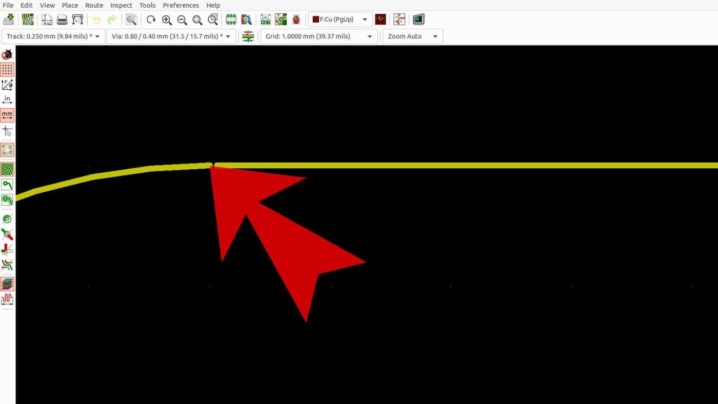
- An outline must be a closed shape, but sometimes a segment of the outline is missing. We either can’t see it because the gap is too small or it’s hidden from us by another feature. It’s worth making sure that your EDA tool’s Design Rule Checkers (DRCs) will flag these problems. Or, manually go over the outline zoomed-in to look for any anomalies, like kinks and stubs, that are hidden because of the viewing scale.
- Sometimes other information sneaks into the outline layer either by the designer or the EDA tool, and that information is then present in the data that we supply the manufacturer. This can cause a lot of confusion. I highly recommend making sure to only include outline information in the relevant layer. If you need to convey something to the manufacturer, do that in the mechanical- or other user-layer.
Manufacturing considerations
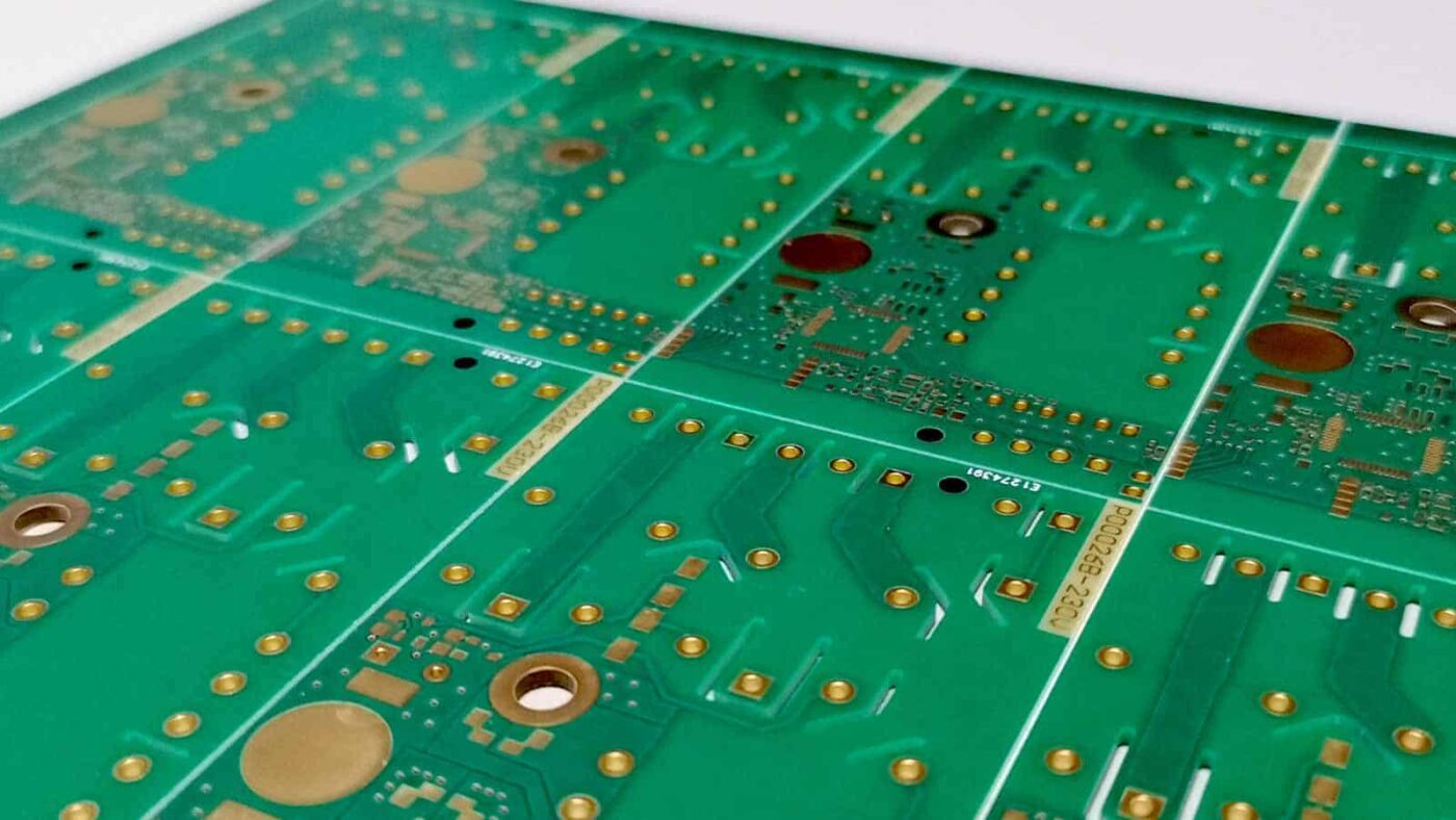
Boards are manufactured on a panel that holds several instances of the same board or several different boards such as with ‘pooled’ services. Individual boards are cut out of a panel using a router that goes along the contour of the board. Or, two sharp knives score the board from both sides (‘V-cut’) and then later snapped-out of the panel; the two techniques can also be combined in the same design. V-cut can only go in straight lines that are either parallel or perpendicular to a rectangular panel, and consumes very little panel space. A router can do almost any arbitrary shape, although it ‘spends’ its diameter in material as it goes. Both methods require sharp and robust tools that will create an acceptable edge without causing damage to the board.
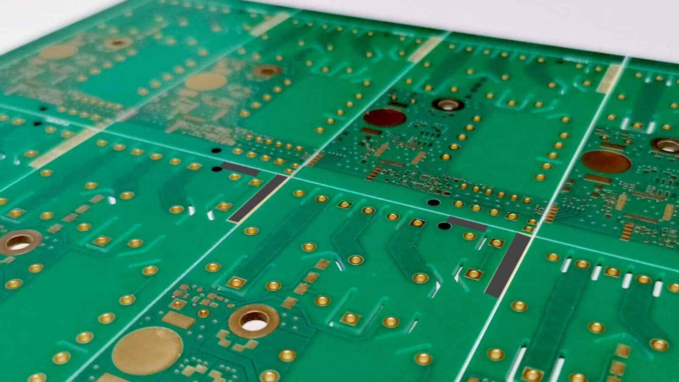
Dull tools can cause haloing where the base laminate fractures and loses its integrity, or leave behind burrs, tiny excess material on the surface or edge of the cut.
Routing-out the boards from the panel is one of the last steps of PCB manufacturing, but often we’d like to keep them just barely attached to the panel so it’s more convenient for assembly of components. To do this we keep the boards attached using ‘tabs’, or ‘mousebites’, that hold the boards onto the panel. When they are ready to be shipped those tabs can be easily broken, ideally leaving as little material as possible on the edge’s surface.
All of this requires consideration by us designers to make sure that our data is unambiguous so that the manufactured boards have as few faults as possible.
- The machine that routes-out the boards has a specified accuracy tolerance, or ‘registration’, so we need to keep an area of a certain distance from the outline clear of anything other than soldermask. This distance will be specified by the fab house and the standards you’re following, and it’s good to find out what those are early on.
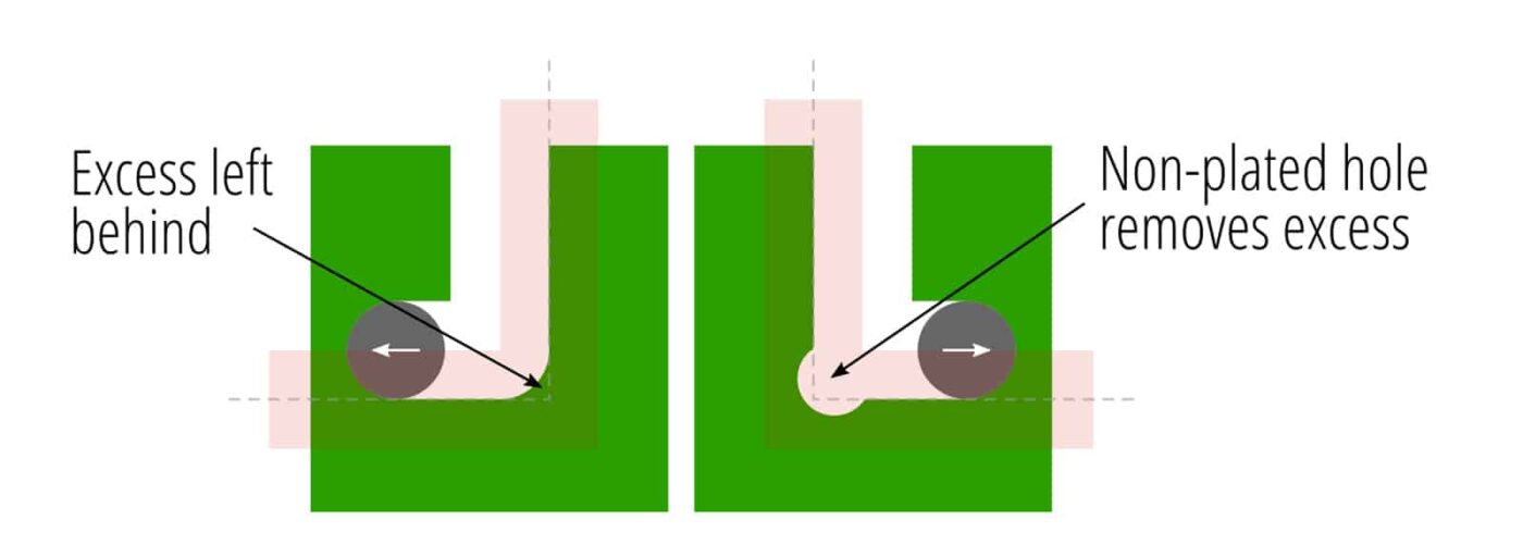
- The most common routing bits are 2mm in diameter, which gives us a 1mm radius corner. For smaller radii you’ll need to find out if the manufacturer is capable of it. In most cases you’d need to specify this requirement explicitly; otherwise they’d use their standard bit and leave the excess there. But you’re able to sidestep this limitation, and perhaps also avoid higher costs, by placing a non-plated hole at the corner to take away the excess.
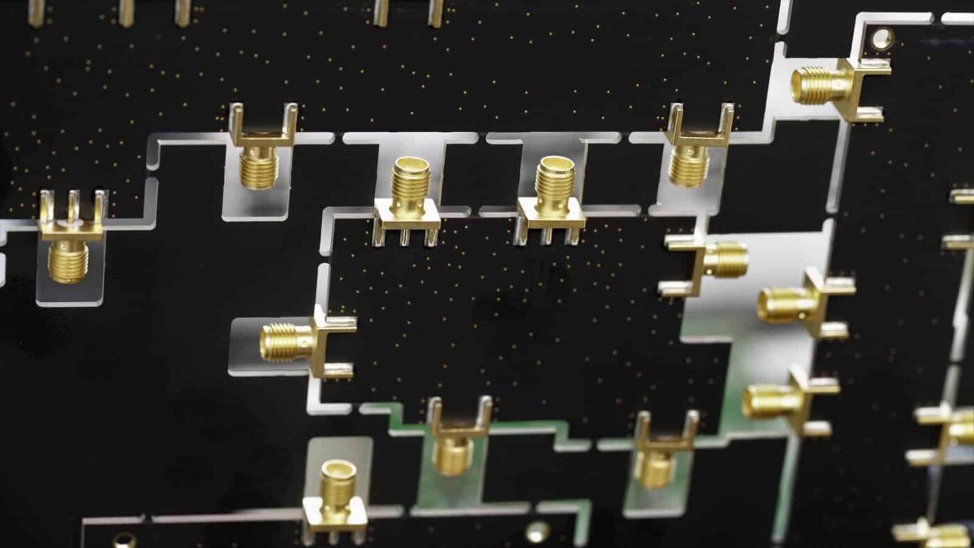
- Components hanging over the edge are fine as long as they are not hanging over a break-tab, a situation that may result in two undesirable things. Firstly, the component might not sit flush with the PCB because it is propped up by the tab (good examples are micro-USB connectors that have a bottom ‘lip’ that goes below the surface of the board, and edge-launch SMA connectors that are mostly hanging off the edge). And secondly, breaking the tab might lift the component, weaken its joints or even break it off the board. It’s almost always a good idea to ask the manufacturer whether to supply tabs or not, and let them add the tabs because they have the experience and tools to do it best.
So far we’ve discussed the topic in general terms and we hope that this information would help you get great boards back, no matter where you manufacture them. But, of course, we’d be happy if you use us for your boards! Here’s how our way of doing things helps you get it right the first time.
How the Eurocircuits way helps
Our PCB Visualizer is a powerful tool that helps both you and us get it ‘right the first time to manufacture’, which is also our motto. The Visualizer is what you’ll use during the ordering process to make sure everything is good to go.
In the case of outlines the Visualizer will alert you of misaligned or incomplete outlines if it cannot fix them itself with confidence. You’ll then either be able to fix these within the Visualizer using the ‘Outline Editor’, or upload new files. We’ll also measure and report any issues with pads or tracks being too close to the edge of the board. If we withdraw other copper regions from the edge in order for them to meet the spec, and that causes a net open, we’ll also report back. You’ll need to fix those issues in your design. You can also tell us of specific copper features that need to reach the edge of the PCB and we’ll accommodate that. Be aware, however, that UL prohibits any copper to reach the edge.
Designers sometimes include the outline in every layer that’s sent to us for manufacture. This used to be a good idea for aligning things, but now it’s a nuisance because we need to remove it from every layer and that can result in ambiguities. When you send us your design files please have the outline only in one dedicated file, but also verify that orientation, mirroring, registration, and offsets of all the files in the set are also correct.
Our standard routing bit for outlines is 2mm. If you require use of smaller bits in your design please specify it in a mechanical layer. If you select ‘customer panel’ — where you design the panel — as your delivery form and choose to use V-cut for pre-cutting, we will use this technique instead of routing.
You can use our Visualizer as your ‘external’ Gerber viewer; we work closely with Ucamco to implement the latest Gerber improvements. And finally, when you place an order you can also choose Post-Production Approval (PPA) so we’ll alert you to approve the files that are ready for production and only then we’ll proceed to manufacturing.
Here are our resources for the specs that are relevant to what we’ve discussed so far:
- Eurocircuits’s copper clearance from the edge
And in the case of UL-marked boards - Routing and milling information
- Overhanging and heavy components information
- Complete guide to panels
Bring your product to market on time and within budget – join the Eurocircuits Community


![]()

