
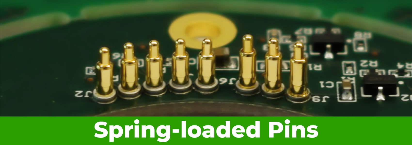
Sometimes our electrical connections need to be solid, but temporary; or, it is subjected to enough vibration to undo it; or, we need to make or break many connections at once, all over the board. In those cases, the usual combination of sockets, plugs, and cables may not be ideal, so we might consider spring-loaded pins or connectors (widely known as ‘pogo’ pins which is, interestingly, a trademark of Everett Charles Technologies).
Spring-loaded pins can bring the following properties to our connections:
- Using pressure, multiple connections can be created or broken at roughly the same time across a large area; very useful for testing jigs – such as bed-of-nails – that need to connect-test-disconnect quickly.
- They require soldered components only on one of the two boards (often the one that isn’t mass-produced); usually, the mating side only needs a small pad at the same place. This saves space, routing area, and cost.
- If chosen and designed well, they can work in an environment with vibrations.
- The compressed connection can be compact vertically; boards can be stacked quite close to each other.
- Springs allow for some height flexibility; this is helpful in the case of uneven boards or staggered board stacks.
Very useful, but anyone who has tried to spec spring-loaded pins or connectors knows that there are nearly infinite combinations of options to choose from: height, diameter, tip geometry, material, plating, stroke, force, housing, and many more. Here we’ll focus only on the properties that are relevant to compatibility with automated component placement and manufacturing. With this knowledge you may be able to avoid components and testing strategies that seem good at design-time, but that may be complex, unreliable, or costly to manufacture later on.
Getting it Right

Two main types – out of many – of spring-loaded pins and what each bit of their construction is called. The ‘pin/tail’ helps make a robust perpendicular positioning; the various ‘termination’ types are for attaching cables (crimp, wire-wrap, solder, etc.). Not shown here are ‘edge’ spring-loaded pins that are placed perpendicular to the edge of the PCB instead of to its surface.
Electrical connections need to be robust and reliable. For that the spring-loaded pin needs to be placed at the ideal angle, be well aligned with the centre of the contact on the other side, and not bend, buckle, or go out of alignment with the applied pressure. The contact pad opposite the pin needs to be flat, large enough to account for alignment mismatches and vibrations, and plated such that the contact doesn’t degrade with use, and time. (Sometimes the contact isn’t a pad, but another component, in which case the spring loaded pin’s properties – like the tip and stroke – may need to change.)

Spring-loaded pin arrays usually come with ‘housing’ or ‘support’ for soldering and alignment. Many, but not all, will come with a ‘cap’ so that a pick-and-place machine can grab the array. Single pins sometimes do not come with housing or caps, making them impractical for pick-and-place.
The component placement, as we know, can be done using an automated pick-and-place (P&P) machine, or by hand. P&P is usually cheaper for high-component-count boards or if more than a few are assembled. So, ideally, we’d always try to choose components that are compatible with this process. When it comes to spring-loaded pins, it’s essential that they have a ‘cap’ which sits on top of each discrete pin, or on a subset of the pins in a ‘housed’ connector array; this cap is what the P&P head grabs onto for placement. Then, they should come in a packaging that’s P&P compatible (tube, tape, reel, tray, etc.) If they are delivered ‘loose’ or in ‘bulk’ the assembler will need to manually put them into a P&P feeder, or hand solder them, and will charge you for the extra work.

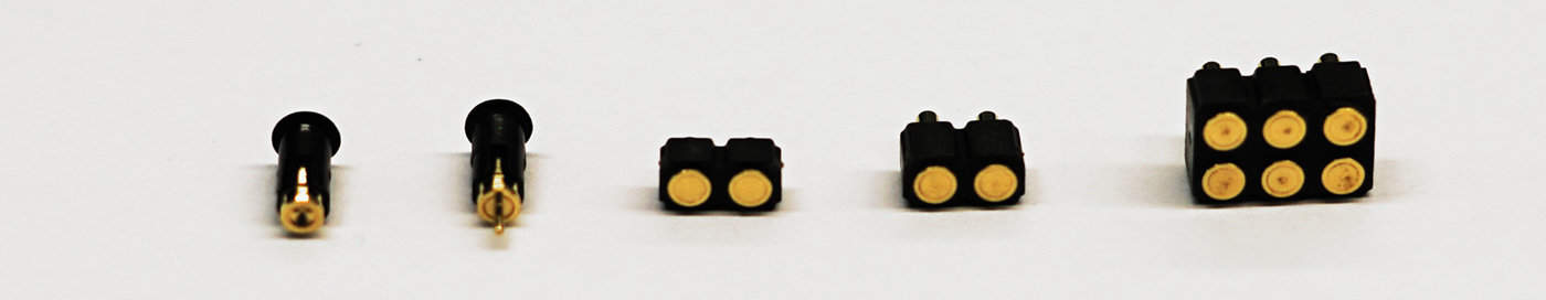
Various types of spring-loaded pins. The two on the left are single pins with a ‘cap’ for placement. The rest are ‘housed’ arrays of pins.
Now let’s address alignment and stability. Here there are important properties:
- Surface-mount or through-hole. Through-hole – for spring-loaded pins this is sometimes called a ‘tail’ – provides a solid solder joint and stability.
- Single or connector array. Single pins, especially ones without housing, can experience misalignment during assembly and stability issues during use.
- The configuration of the ‘connector’ array. A single row (1-by-n) may also experience misalignment when soldered, so a good choice would be a 2-by-2 array or larger. So if there’s a choice between a 1×6 or 2×3 pin configuration, the latter is better.
- Base-area to length proportion. The longer a pin is, or the smaller its base area is, the greater the chance of misalignment and unreliability. It’s difficult to define how long is ‘long’, but it’s something to pay attention to, particularly for surface-mount pins.
The best spring-loaded pin for assembly, in terms of alignment and stability, is therefore: through-hole (with a ‘tail’), as short-as-possible, arranged in a housed 2×2 or larger configuration. If the pin you want to use is ‘long’ or surface-mount, particularly for single-pins, it’s best to consult the assembly-house first to see if they’d have problems with it given their process and equipment.
Single pins are very convenient to design in because the contact pad opposite can be placed right next to the signal, and that saves valuable routing space. But… they can be a source of a lot of problems. They do not always come with caps, are difficult to align during soldering, have a greater chance of misalignment under pressure because of lack of support, and require special assembly jigs that are custom-made for each design, which increases costs.
Finally, always follow the manufacturer’s instructions for assembly and consult them on choosing the best variant for the application… they will help you contend with the overwhelming amount of options and parameters.
Spring-loaded Pins at Eurocircuits
The ideal pin for our pick-and-place process has the following properties:
- Comes in a housed array (ideally in dual-row, 2×2 or greater, for best for vertical alignment and stability)
- Through-hole (either the pins have a ‘tail’ or they have housing that has alignment pins)
- Proportionally ‘short’ relative to its base area
- Comes with a cap (if there’s no cap, we always hand-solder)
- Delivered in tape or reel (we may re-reel if possible and efficient, or place manually)
Sometimes, we know, it’s not possible to use or source the ‘ideal’ pin as above. We’re happy to accommodate all other variants, of course, but it usually means that there will be an additional cost (for hand placement, custom jigs, re-reeling, etc.). As always, in case of doubt we always recommend contacting us early in order to discuss how we may handle your choice of components so that assembling your boards can be done efficiently and cheaply.
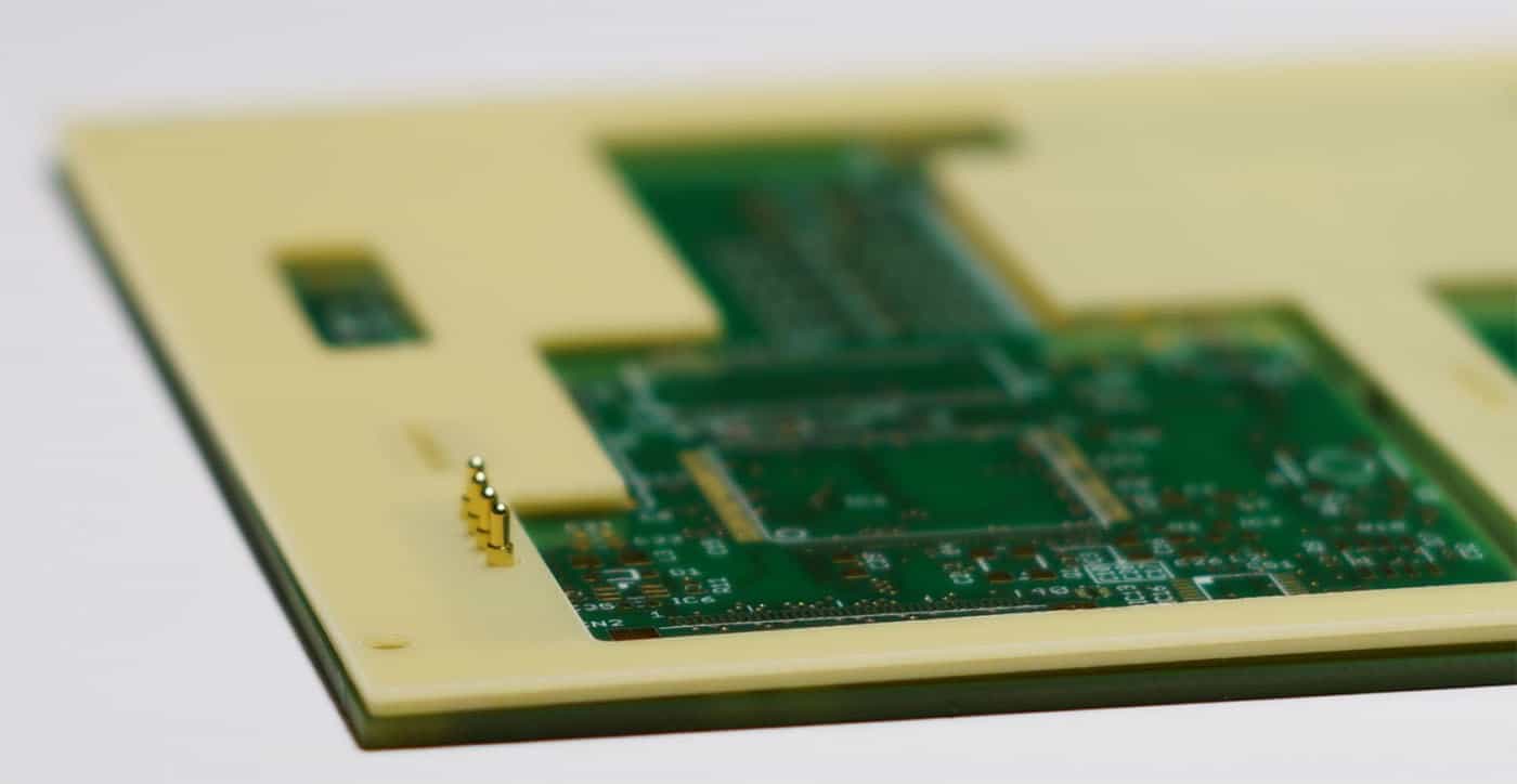


For single spring-loaded pins we create a custom jig to hold them in place.
Be aware that pins that require plated holes of 0.45mm diameter or smaller require special considerations. In our manufacturing process if a plated hole isn’t identified as a components plated hole and has a finished diameter equal or smaller than a certain size (0.45mm is our default default), it is treated as a via. For vias we allow higher ‘negative tolerance’, compared with component holes, which means that the resulting holes may be smaller than the specified size (to accommodate a better annular ring or to optimise the number of drill diameters, etc.).
The safest way to prevent component plated holes from being treated as vias is to lower the threshold for via classification. This is done through the ‘Holes <= [less than or equal] may be reduced’ option (see image below); choose the diameter that’s less than the finished hole diameter required for the component plated hole (for example, if the hole is 0.4mm, choose 0.35mm).
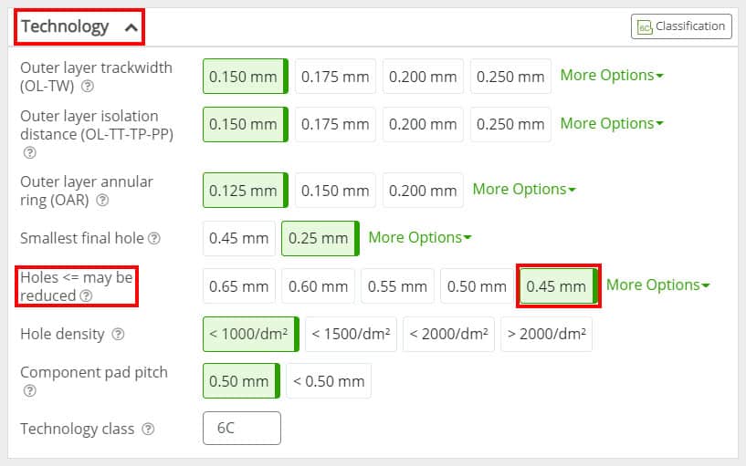
If the ‘through-holes’ for components need to be 0.4mm, choose 0.35mm for the indicated option. Otherwise, they may be recognised as a via with no ‘negative tolerance’.
If we’re doing the assembly for the PCB, when you provide complete assembly information we’d be able to identify which holes are associated with components and then not treat them as a via. This information can be made available through the data you upload (Gerber X2 or later, for example) or specified or verified through our Visualizer.
Be the first to read all about our news and information. Follow us on


