Blogs

Tips & Tricks

Copper-Fills-Featured-Image
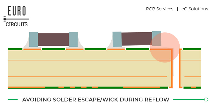
Copper fills – mechanically speaking

This is the sixth and final article of this series about PCB design and manufacturing topics. I hope that you’ve enjoyed it and will continue to follow up on our other publications until we return with series 2! Copper fills — or copper pours — are one of those topics that’s deceivingly simple, but their […]

Fiducials-Featured-Image
Finding fiducials

This is the fifth in a series of articles where we discuss important topics in PCB design and manufacturing. Please follow us on social media and sign up to our mailing list to get our publications. Fiducials are markers that are used as a reference for placement or size; their name, interestingly, is derived from […]

On-the-keepouts-Featured-Image
On the keepout

In this fourth article of our series about PCB design and manufacturing issues I’ll discuss keepouts, a design tool that when used correctly can save us from making costly mistakes. Keepouts are areas of the board where we ask our design tool to enforce some restrictions on what can and cannot be contained in that […]

Understanding-Annular-Rings-Featured-Image
Understanding annular rings

We’re back with a third article in a series of six on PCB design and manufacturing topics. Don’t miss our future publications by following us on social media and signing up to our newsletter. Now let’s talk about annular rings. A very common feature of PCBs is an exposed round pad with a hole at […]

Courtyards-Featured-Image
Good courtyards make good neighbours

We continue our series on PCB design and manufacturing topics; this is the second article of six. Please follow us on social media or sign up to our mailing list to continue getting our publications. Now for today’s topic! When designing boards we naturally first focus our attention on electrical functionality. But we also need […]

Lets-Talk-About-Outlines-Featured-Image
Let’s talk about Outlines

Hello! This is the first article in a series of six where I cover PCB design and manufacturing topics: outlines, courtyards, annular rings, keepouts, fiducials, and copper fills. We will publish the series weekly as part of our ongoing Technology Thursday publications. To make sure that you don’t miss them please follow us on the […]

Defined-Impedance-Calculators-Featured-Image
Defined Impedance Calculators

There are many different Impedance calculators for PCB designers to use, some are free such as the one available to Eurocircuits customers and some you need to pay for a licence or a monthly subscription. The aim of them all is to provide the necessary track/gap and isolation values for the layout and manufacture of […]

Selecting-the-right-surface-finishes-Featured-Image
Selecting the Right Surface Finish for Your PCB

To protect the copper solder pads on a PCB from oxidation, contamination and to enhance their solderability, they need to be protected with a Surface Finish and these must conform to the European Union RoHS & RoHS2 (Restriction of Hazardous Substances) Directives. But which is the right Surface Finish for your PCB’s? In accordance to […]

Tips & Tricks – Why Do Components Tombstone

Ever wondered what is Tombstoning and why does it happen? What is Tombstoning? Tombstoning also known as the Manhattan or crocodile effect is where one end of the component lifts from a pad of the PCB during reflow soldering process and affects mainly surface mount components such as resistors, capacitor and inductors. Why does it […]

Avoiding solder escape/wick during reflow
Tips & Tricks: Avoiding Solder Escape/Wick during Reflow

Have you ever wondered why sometimes you have poor Solder joints on your PCBs? One of the main reasons is that the Solder Paste flows away from the pad on the PCB during Reflow, this is known as Solder Escape, Solder Wick or Solder Drainage. Why does this happen, well there are a few reasons […]

Eurocircuits launches SMS messaging for time critical orders !

Eurocircuits launches SMS messaging for time critical orders Whenever you are in need of a very fast turn around time for your PCB order or when you have a critical delivery to be made and you want full instant control of the production flow of your board, you can initiate SMS-massaging for your order. By […]

Blind and Buried Vias

Blog post byDirk Stans/28 September 2016 Blind and Buried Vias Blind and buried vias are used to connect between layers of a PCB where space is at a premium. A Blind Via connects an outer layer to one or more inner layers but does not go through the entire board. A Buried Via connects two […]

Other ways to find help

User Guides

Our User Guides provide step-by-step instructions on how to use our free online smart tools and other available software.
View all 5 user guides

Glossary

To simplify communication Eurocircuits uses abbreviations for many of these technical terms. Most of the technical terms and abbreviations are international standards in the Printed Circuit Board manufacturing industry. However to make it clear to everyone involved, we here present a list of technical terms and abbreviations along with their explanation.
View our glossary

Still need help?

Talk to our customer support via our online chat, telephone or email.
Contact us