Plating Index Solutions
Tips and tricks on How to achieve a more even copper density
The basic solutions proposed here for improving the Plating Index focus on copper density spreading.
When designing a board there are several other design specific electrical properties of the board which should be taken into account.
Electrical shielding for EMC or for high-speed or high-frequency boards can lead to the functional use of local or irregular copper planes.
Boards that will carry high voltages or boards with embedded antenna systems may need big isolation areas or copper free areas.
The design challenge is of course to combine the required board specific electrical properties with the below given copper spreading solutions into a workable design.
Finding a good combination is not always easy, but when achieved it will lead to a board design that is not only easier to produce but which also has a better life expectancy in the field.
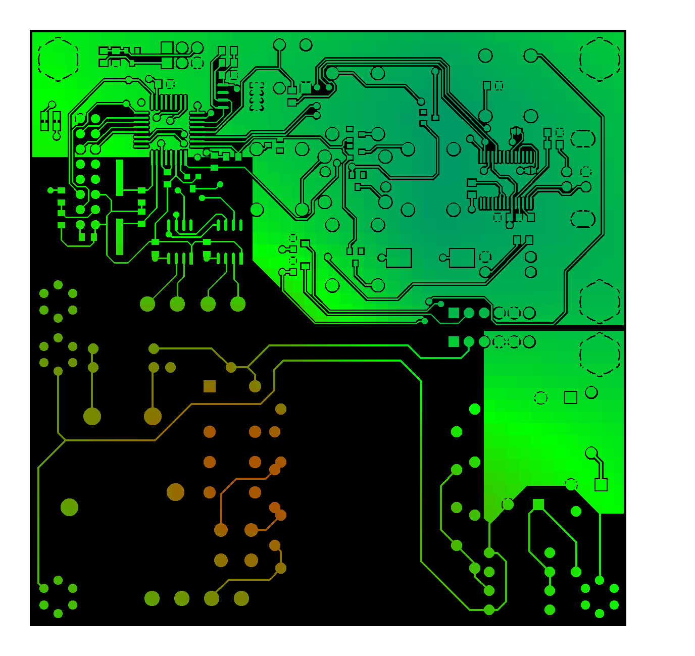
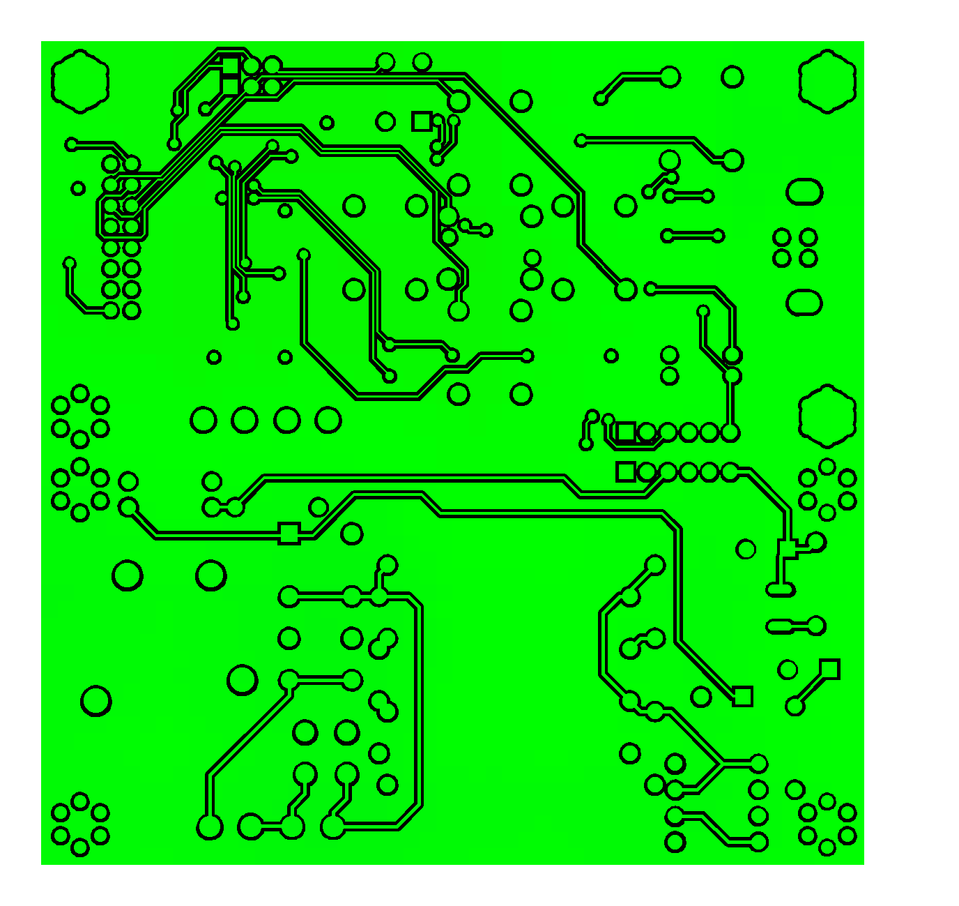
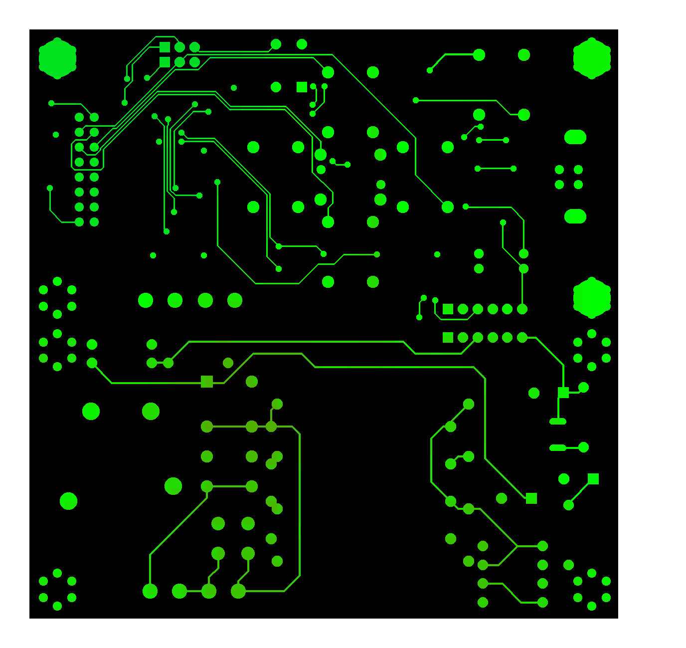
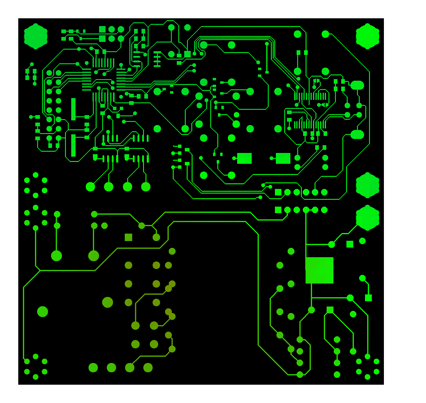
Looking at single boards, there are 2 main solutions to work towards a more evenly spread copper density.
- Add copper to low density areas (Red coloured areas).
Copper can be added as one or more copper plane areas.
We prefer the use of solid copper planes, so that should be the first option to try.
If with solid planes the copper distribution cannot be evenly spread a second option is to use a cross-hatching pattern for one or more areas on the board. Take care when using a hatching pattern, it should comply with the minimum hatching pattern specifications (see our PCB design guidelines)
| BAD | |
 |
 |
| GOOD | |
 |
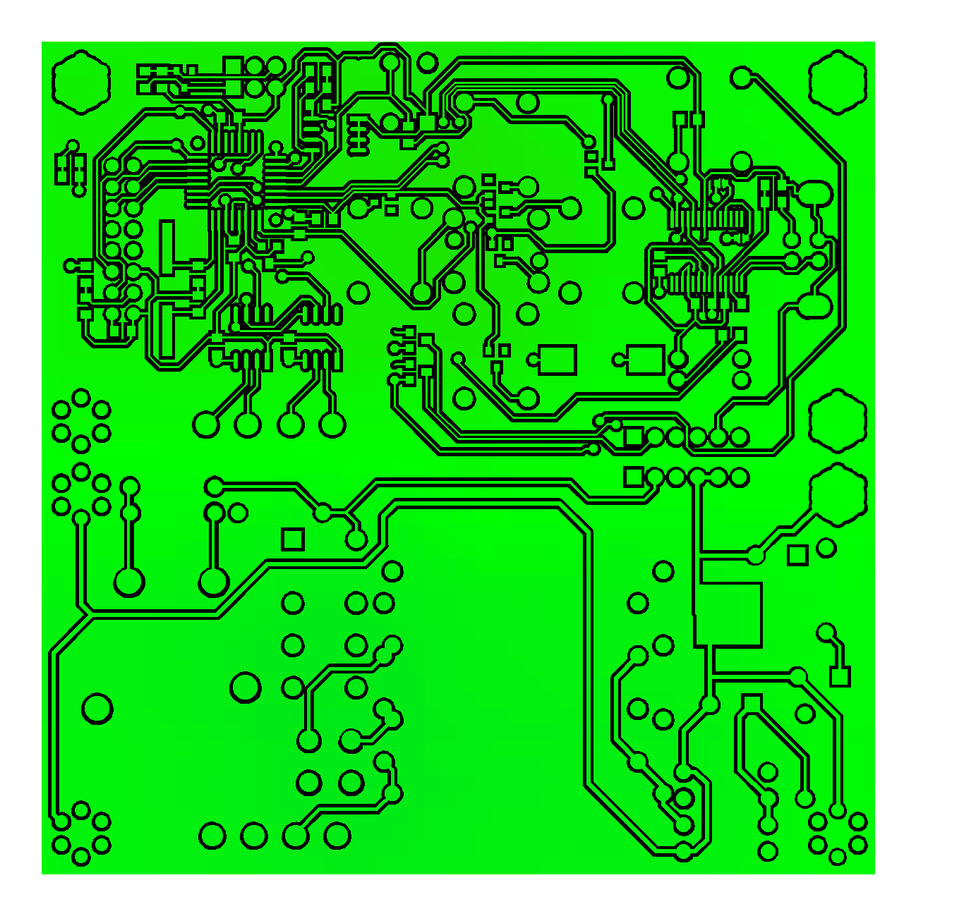 |
- Remove copper from high density areas (Blue coloured areas).
A local solid plane can be replaced by a cross-hatching pattern to create a more evenly spread copper distribution. Here again, take care of the minimum hatching pattern specifications (see our PCB design guidelines).
Complete redesign or even removal of a copper plane can also be a solution.
| BAD | |
|
|
|
| GOOD | |
 |
 |
For customer panels the solutions depend a lot on the specific panel design, but are in general more straight forward and thus easier to implement.
As designer you can easily prevent PlatingIndex problems on panels by making a good panel design.
Proper panel design in fact starts with a good single board design and ends with a proper panel composition.
If the single board has an evenly spread copper density, then a panel of these boards will also have a good spread.
On the other hand when the panel is composed of several different single boards with different copper spreading’s, it is logical that you will have a panel with a bad copper density distribution.
Below you can find some solutions for fine-tuning your panel designs towards a more evenly spread copper density.
- Add copper to the panel border and the space in between the single boards.
Panels will most commonly have a problem of a low to very low PlatingIndex caused by the extra copper free material of the panel border and the possible areas in between the single boards.
Most often a solid copper plane at these very low density areas will do the trick. In some rare cases a hatching pattern will be the solution.
| BAD | |
 |
 |
| GOOD | |
 |
 |
- Reorganize the position and/or orientation of the single boards in the panel.
If your panel consist of several different boards with different copper densities, or if the boards in the panel have an uneven copper distribution you can try and find a solution by repositioning your boards or giving them a different orientation in the panel.
Also adding some extra space in between certain boards can be helpful, as this space can be filled with a copper plane or pattern to even out the copper spread.
| BAD | |
| |
|
| GOOD | |
 |
 |
- Split the panel in two or more separate panels.
Sometimes live is hard and you come to the conclusion that your effort to try and combine single boards with massive copper density differences will not work out.
Only option left in such cases is to split your panel up in one or more separate panels of single board combinations that have a more or less equal copper spreading.
| BAD | |
| |
|
| GOOD:Split panel1 | |
 |
 |
| GOOD:Split panel2 | |
 |
 |