Slots and cut-outs
Milling, slots and cut-outs – hints and tips.
One of the most frequent questions we get asked via our support services is “how do I define slots in my PCB?”. Slots and cut-outs also generate many exceptions, which may lead to delivery delays. Some exceptions occur because the definition of the slots is not clear; others because slots and cut-outs are in the data but not in the order.
Terminology
“Routing” describes the cutting of the board profile, outline or contour. We use a 2 mm cutter for this. Any feature which can be cut with the 2 mm cutter is part of the profile.
“Milling” refers to any slots or cut-outs inside the PCB, but also to any slots in the profile of the PCB which can’t be cut with a 2 mm cutter.
How do I define my slots?
Gerber mechanical layer.
The safest and clearest way is in a Gerber mechanical layer which shows the slots/cut-outs and the profile of the PCB. Two possible ways forward:
- Use draws and/or flashes with the correct end size of the slot/cut-out
- Draw the slots/cut-outs with a 0.50 mm line. It has the advantage that at the same time the line helps you to visually check the clearance of any copper to the board edge. Our engineers will take the centre of the line as the edge of the slot.
Combine your definition of the slots/cut-outs with the PCB contour (outline) into one Gerber file. This layer should line up with the copper layers, but to be as safe as possible make sure that the copper layers also include the PCB outline.
Different systems have different names for the mechanical layer (for instance in EAGLE it is layer Milling – layer 46). Provided that you have included milling in your order (see below) our engineers will find the right file.
If there is no mechanical layer, you may have to adapt another layer. If there could be any doubt which is the right file, point to it in a README file.
Avoid defining slots only in a copper layer or in a legend layer, as they are then very easy to overlook or misunderstand. You can indicate large cut-outs in a copper or legend layer, but make sure that there is a clear outline, and put text CUTOUT in the middle.
Drill file.
Some CAD systems allow you to define slots in the drill file. This is also safe and clear. But they must be defined as slots with an X & Y dimension, not as a row of overlapping holes.
Plated/non-plated.
We take slots with copper on top and bottom to be plated. Give the dimension of the finished slot size. We will make the necessary adjustments for the plating.
Slots with no copper on top and/or bottom layer are non-plated. If you need non-plated slots through copper pads, indicate this clearly in the mechanical layer or in a separate drill file.
Example:
This pictures shows the customer data:
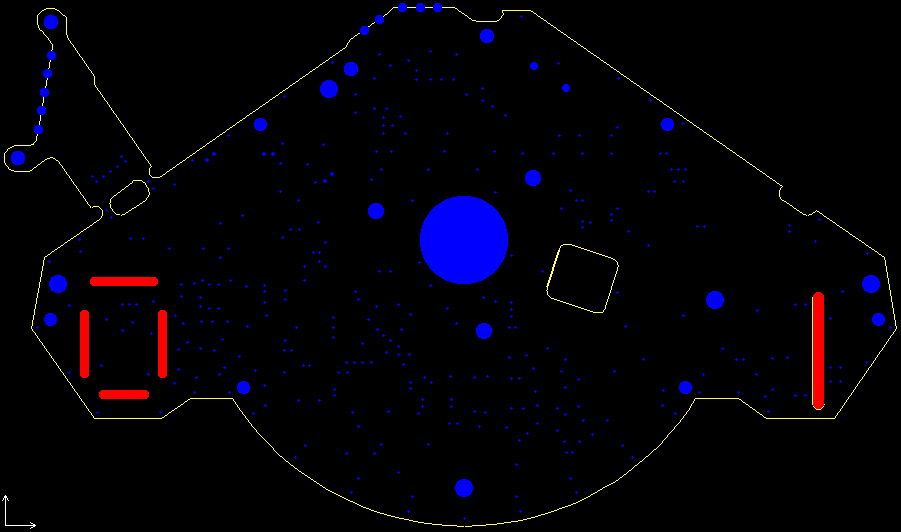
- an outline file containing some cut-outs (contour file, drawn with a 0.50mm line) – yellow
- a drill file containing all drill holes and large round cut-outs defined as flashed hole – blue
- a routing layer containing all slots defined as tracks with the correct slot sizes – red
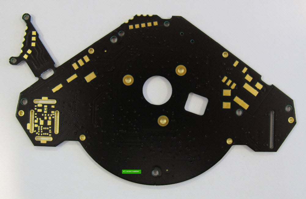
The result shown on the final board. Note also the difference between the plated slot and the non-plated cut-out.
How do I order my slots?
In the Price calculator menu go to the section headed PCB definition and then to the Milling box. There is a choice of 3 cutters: 2 mm, 1.2 mm and 0.50 mm. Select the one which is the same size as, or smaller than, your smallest slot size. Note that you cannot use a 0.5 mm cutter on board thicknesses greater than 2.00 mm.
If your board has slots or cut-outs, make sure that you fill in the Milling box. It alerts our engineers that your board need milling.
1.2 mm and 0.5 mm cutters are cost-options. If they have not been selected, we will need to increase the price of the PCB so our engineers will raise an exception. There is no charge for the 2.00 mm cutter as it will cut the slots at the same time as it cuts the profile – but still complete the box so that we know that you need slots or cut-outs.
How do I check my slots?
PCB Visualizer is an automatic Gerber pre-production analyser. Gerber is a pure vector format with, at present, no built-in attributes. So PCB Visualizer cannot always detect structures like slots and cut-outs. What is possible at the moment:
- Your slots/cut-outs are defined using flashes and/or draws, placed in a separate mechanical layer and this layer lines up perfectly with all other layers => PCB Visualizer has no troubles recognizing all slots/cut-outs and displays them correctly.
- Your slots/cut-outs are drawn with a line (0.50mm). PCB Visualizer will display the line but the material inside the line will not be removed from the image. Our engineers will find and define them when they prepare the tooling for the PCB. Once this is done, you can view the prepared data in PCB Visualizer as the “Production data” rather than the “Customer data”.
If you want to check that the slots and cut-outs are correct before the board goes into production, set up pre-production approval by clicking the “Request pre-production approval box” under Running orders. The job will then be halted after tool data preparation for you to check.
If you have any questions, contact our Live Chat support.