Designing better PCBs: CAM-CAD communication

Speaking the same language is important for communication, obviously, and is particularly so when talking about technical data for manufacturing. PCB data files are generated using CAD – Computer-Aided Design – software that are then sent to a manufacturer, who processes them with CAM – Computer-Aided Manufacturing – software so it’s ready for manufacturing. (CAD is a superset of the more specific EDA – Electronics Design Automation – but here they are interchangeable.)
As the names suggest, CAD is powerful in creating a design but is rather limited in its analysis capabilities (DRC, Design Rule Checks and DFM, Design for Manufacturing). CAM is the opposite: it has very powerful analysis capabilities but quite limited design capabilities, and, of course, it has no real awareness of the electrical functionality of the design (represented as a schematic, which is rarely sent with the data). Another way to put it is that a designer can get a fully functioning physical PCB back from the manufacturer whilst knowing little or nothing about the manufacturing process.
PCBs are routinely made without the designer ever talking to the manufacturer; this is possible not because the PCB data (Gerbers, etc.) is perfect, but more because the CAM side has learned to more-or-less guess the intentions of designers. This is a coping mechanism of the CAM industry for dealing with poorly or partially implemented specs, CAD/EDA software bugs, and a huge variation in the quality of data that they get. The guessing is also there because, as mentioned, the designer is mostly disassociated from the manufacturing details. And because of this, sometimes things go wrong.
Good manufacturers try to minimise the guessing and return to the designer with some observations and questions about the data, often with suggestions for fixes (we call it Data Feedback); they try to do this sparingly because it causes delays and may annoy the designer. This feedback has a big advantage, though, as it lets the designer correct any issues on their end, so it isn’t an issue in future exchanges. But this communication has a slight problem: whilst the data is essentially the same, CAD and CAM look at it with different eyes, and speak of it in somewhat different languages.
A couple of examples where things differ
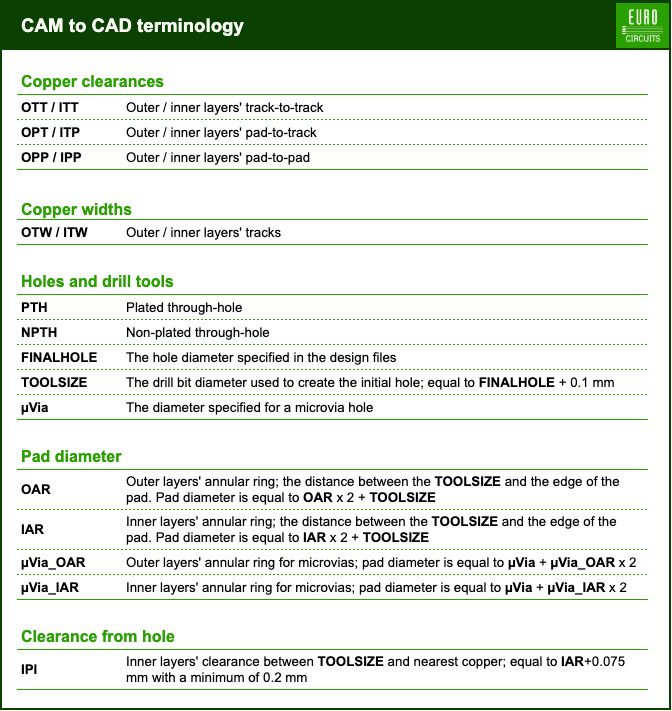
PCB designers mostly care about a single clearance parameter: distance between copper of different signal nets. This parameter applies to any copper feature whether it’s a track, pad, or plane. Manufacturers, however, break this parameter down to several types of clearances, and this is the basic level on which their CAM software reports its analysis results. The various sub-categories of copper clearances that Eurocircuits uses are shown in Figure 1; the first split is for outer and inner layers and then distinguishing the distance between specific copper features. This is essential because manufacturers may treat each of those sub-categories differently; for some of them they may be able to make minor tweaks to have the design pass their checks, and for others they cannot; and, for some, they may be able to be more forgiving. That’s all based on their expertise and experience with their manufacturing details.

When it comes to (round) pads designers normally care about the smallest diameter possible for the technology they are using. This diameter allows quick evaluation of whether vias are going to fit somewhere or if a track will fit between component pads. As before, the CAM view is more complicated since manufacturing a hole with a pad around it isn’t as simple as defining them in the data!
CAD usually talks about pad diameters, but CAM likes to define them as an ‘annular ring’, which is not a diameter, but the pad diameter minus the drilled hole diameter divided by two. So how do we go from one to another? In order to manufacture a conductive hole, like a via, they must drill a bigger hole in order to account for the thickness of the plating of the barrel of the hole. This is where TOOLSIZE comes from: it’s the drill diameter used to create the hole and is equal to FINALSIZE (the diameter defined in the design) plus 0.1 mm (for the plating). Finally, this means that in order to get to ‘smallest possible pad diameter’ we need to add twice the annular ring, plus the TOOLSIZE (not FINALSIZE!). (Oh, non-plated holes are simpler since TOOLSIZE and FINALSIZE are the same.)
For even more fun, microvias are different because some of them are filled with copper (in our HDI pool, L1-L2 vias are filled with copper whilst the L2-L3 are plated and filled with resin). For these vias there’s no TOOLSIZE when figuring out the pad size from the annular ring; and, sometimes, there’s no hole remaining on the board itself, even though a hole is defined in the data! This is another example of the manufacturing realities that are often opaque to the designer.
How to design better boards?
We become better PCB designers the more we understand the details of the manufacturing process since it gradually becomes part of our thinking and workflow. The results are better DFM, faster turn on boards, and cost savings. The first step in familiarity is learning some of the language PCB manufacturers use in order to understand their guidelines and feedback better. Bridging this gap takes a bit of effort but is worth its returns.
Gehören Sie zu den Ersten, die unsere Neuigkeiten und Informationen erhalten. Folgen Sie uns auf


![]()

