Designer Insight: partial HDI PCB differential signals FPGA routing
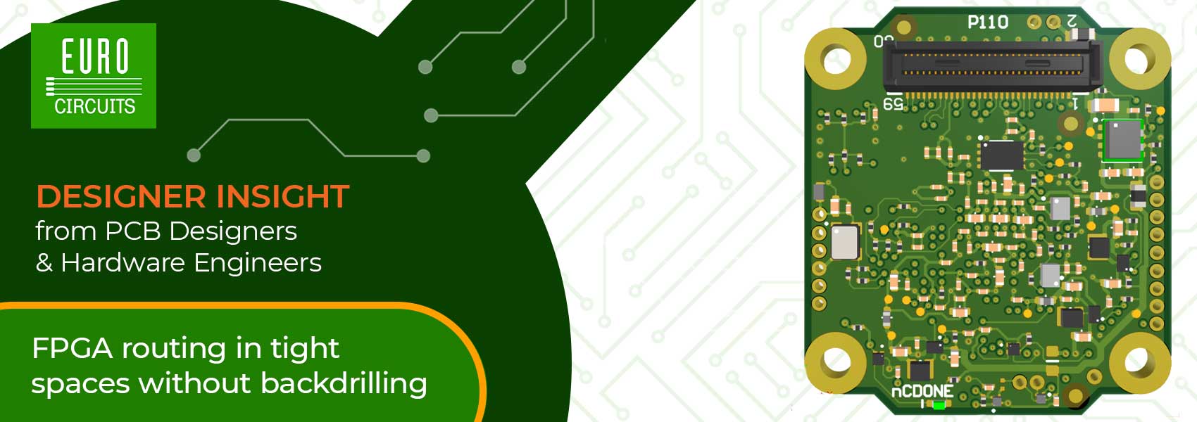
#1 Design of an FPGA module for video signals
👤 About the Author
Frank R., CID + FED Designer
📍 Germany
🎯 Focus: demanding High-density layouts (High speed design)
“Signal integrity starts with clean layer transitions.”
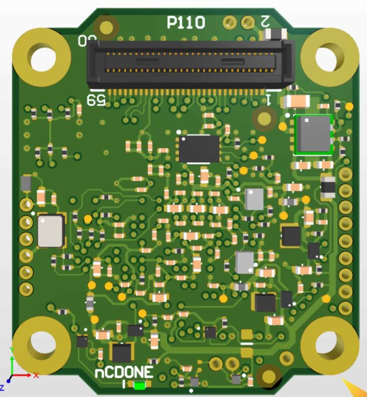
📦 Project Overview
Design of an FPGA module for video signals
📏 Severely limited installation space
⚡ High-speed differential signals
📐 Precise track length matching required
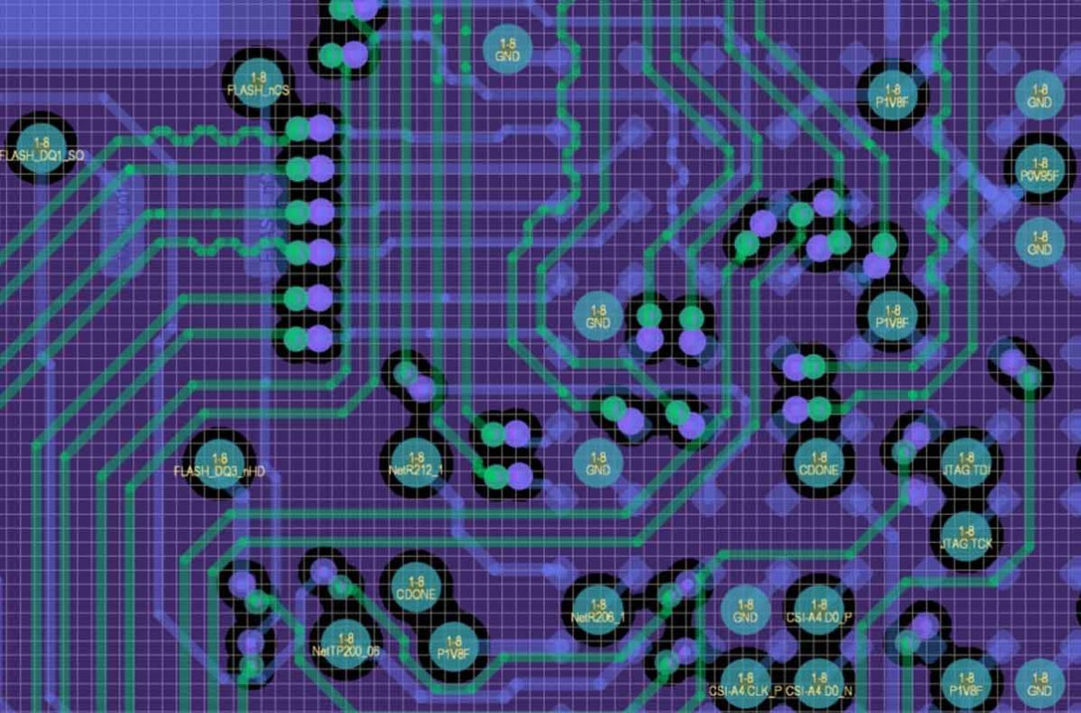
⚙️ Technical Challenge
💡 Objective:
Achieve space-saving routing of differential video signals without backdrilling and without compromising signal integrity.
Design constraints:
- Vias without stubs
- Via areas used exclusively for active signal layers
- Remaining layers fully available for length matching
- No routing restrictions caused by through vias from other layers
Key layout decision:
The fastest signals were routed from the outer layer to the layer directly below it, sharing the same reference plane.
✅ Benefits:
- Selected GND stitching vias could be omitted
- Additional routing space gained
- Extensive length matching possible despite limited space
- No backdrilling required
The small footprint of microvias prevented differential pairs from being forced apart contributing directly to improved signal integrity.
🧩 Engineering Strategy
🔬 Targeted use of “Partial HDI”
- Microvias only where they create real value
- No unnecessary HDI complexity
- Maximum routing density with controlled process effort
High density manageable manufacturing complexity.
🏭 Eurocircuits Contribution
🚀 8-layer pooled build with “Partial HDI”
- Limited additional processing on one inner core
- Fast prototype turnaround
- Cost-efficient implementation
🔍 Design Review in the PCB Visualizer
During the review:
- Deviations in BGA pad sizes were detected
- Compared against reference data
- Corrected and aligned for both library and project
👉 A potential production issue was eliminated early.
📊 Result & Benefit
✅ Low-cost, fast prototype production
✅ Clearly defined and stable signal behavior
✅ No backdrilling required
✅ First version worked immediately
Strategic advantage:
“Partial HDI” is also suitable for later cost-efficient series production, as it requires fewer process steps than a fully double-sided HDI solution.
💬 Designer’s Opinion
“The Eurocircuits HDI pool solution enabled us to achieve the required project costs and timelines. Thanks to the PCB Visualizer reviews, the first version went into operation immediately.”
🎯 Engineering Principles from This Project
💡 Use microvias strategically not universally.
Apply HDI where it improves routing density and signal quality.
💡 Plan layer transitions under a shared reference plane.
Clean reference control saves stitching vias and creates routing space.
💡 Think ‘Partial HDI’ before going full HDI.
Targeted complexity often delivers better cost-performance balance.
💡 Verify footprints before production release.
Library and project data must match before it becomes expensive.
Bring your product to market on time and within budget – join the Eurocircuits Community


![]()

