Why standardised buildup
For many PCB designs, a proven and standardised buildup reduces engineering effort, improves repeatability & reproducibility and simplifies the transition from prototype to series production.This also allows the development teams to focus on what really creates value: the design itself.
A new project starts. The requirements are clear, the schematic is taking shape and someone asks a familiar question: “What buildup are we going to use?”
Printed circuit boards occupy a unique position in electronics development. Unlike resistors, capacitors or integrated circuits, which are manufactured in large quantities with fixed specifications, a PCB is usually designed and manufactured specifically for a single product.
Every PCB reflects engineering decisions, application know-how and, ultimately, the intellectual property behind the product.
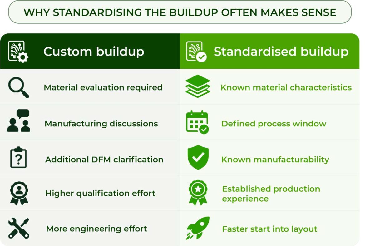
Because every PCB is unique, many engineers assume that each new design also requires a new buildup. In practice, however, this is often where valuable development time is lost. For many applications, a proven and standardised buildup will provide all the required electrical and mechanical performance while significantly reducing engineering effort and cost.
Start with the design
Most development teams work under the same constraints: time and cost. Engineering resources are limited, project schedules are tight and every design decision consumes effort.
The challenge is deciding where that effort creates the greatest value.
For many projects, competitive advantage does not come from a custom PCB buildup. It comes from functionality, performance, reliability and the benefits the product brings to the customer.
A designer’s expertise is usually far more valuable when applied to circuit architecture, signal integrity, thermal management or product functionality than to redefining manufacturing parameters that are already well understood.
This is where standardisation becomes a powerful engineering tool. Instead of spending valuable engineering hours evaluating material combinations, defining layer structures and reviewing manufacturing constraints, designers can focus on the actual development work. The project starts with the design rather than with a manufacturing discussion.
Why standardisation makes sense
Standardisation is sometimes perceived as a limitation on engineering freedom. In reality, it often achieves the opposite. Every development project contains hundreds of decisions. Some directly influence product performance and differentiation. Others simply define how the product will be manufactured. Good engineering is not about maximising the number of decisions. It is about identifying which decisions truly matter.
For many PCB designs, a proven, standardised buildup provides exactly that advantage. Instead of starting from scratch, designers can build on a manufacturing framework that has already been validated. The electrical behaviour is understood, the materials are well characterised and the manufacturing processes are optimised.
The result is less time spent defining the PCB construction and more time spent designing the product.
The value of manufacturing experience
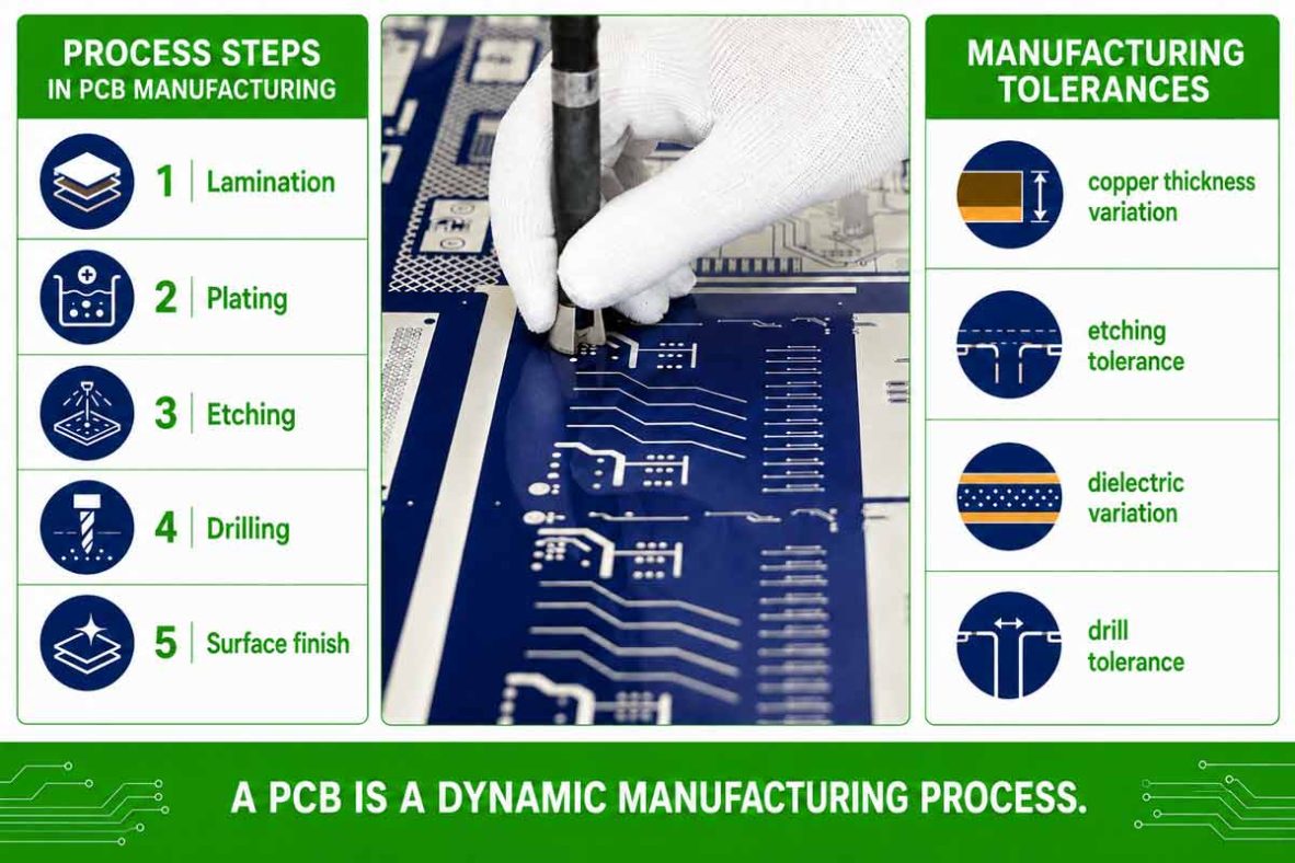
A PCB is far more than a carrier for components. It is a complex construction made from different materials and produced through a sequence of chemical, mechanical and thermal processes. Copper is plated and etched. Layers are laminated under heat and pressure. Holes are drilled and metalised.
Each process introduces unavoidable tolerances. Copper thickness changes during plating. Track widths are influenced by etching. Material thicknesses vary during lamination. Electrical material properties are specified within defined ranges. These variations are normal. The key is to understand and control them.
This is where proven buildups offer another important advantage. When a PCB manufacturer repeatedly uses the same materials and layer structures over thousands of production orders, their behaviour becomes highly predictable. Process windows are understood. Material performance is known. Electrical characteristics become more reproducible and reliable.
What designers gain is not merely a predefined buildup. They gain access to years of accumulated manufacturing experience. That experience translates into more predictable results, fewer surprises during production and greater confidence that the first prototype will behave as expected.
Faster development, easier upscaling
The benefits become visible from the very beginning of a project. Using a standardised and proven buildups reduces the number of technical decisions that need to be made and shortens the path from concept to layout.
The advantages continue when a design moves beyond the prototype stage. Products based on established materials and manufacturing processes are generally easier to upscale into series production because their behaviour is already well understood. Material availability is known, process capability has been proven and additional qualification effort is often reduced. For start-ups and lean development teams, this can significantly reduce both risk and time-to-market as well as costs.
A practical approach
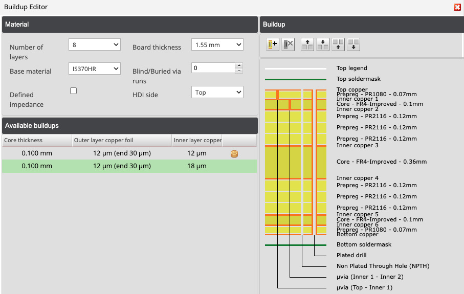
At Eurocircuits, this philosophy is reflected in our pooling services and Buildup Editor. Instead of starting from a blank sheet, designers can choose from more than 900 predefined buildups based on proven materials and established manufacturing processes.The goal is not to restrict design freedom.It is to standardise where standardisation creates value and leave engineers free to focus on the areas where innovation actually happens.
Every PCB is unique.The product requirements, functionality and intellectual property behind the design will always be different. But that does not mean every aspect of the PCB needs to be reinvented. In many applications, a standardised and proven buildup is not a compromise. It is simply the smarter engineering choice.
Bring your product to market on time and within budget – join the Eurocircuits Community


![]()

