Electroless copper deposition

Note

This process is no longer used and has been replaced by the the Black hole process.

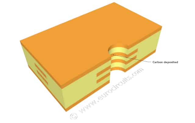
The first step in the plating process is the chemical deposition of a very thin layer of copper on the hole walls.  The operator clamps the production panels into the jigs.  The line is fully computer controlled and the panels are carried through a series of chemical and rinsing baths by the overhead crane.  Almost all PCBs with 2 or more copper layers use plated through holes to connect the conductors between the layers.  A good connection needs about 25 microns of copper on the walls of the holes.  This thickness must be electroplated, but the walls of the holes are non-conductive glass cloth and resin.  So the first step is to deposit a conductive layer over the hole walls.  We use electroless copper, that is we deposit chemically a layer of copper about 1 micron thick over the walls of the hole (and incidentally across the whole panel).  This is a multi-stage process as you see from the video with washing steps between the stages.  We pre-treat the panel, then we seed the hole wall with micro-particles of palladium, and finally deposit the copper


Return to the process overview – Making a PCB – PCB Manufacture step by step

< Prev    Next >