
PCB Outline: The most frequent mistakes in PCB data

The PCB outline is one of the most basic elements in a design and still the most common DRC-related issue. The PCB outline appears geometrically complete and visually correct in the design tool.
However, small inconsistencies such as gaps, overlaps, or conflicting segments may remain undetected by the CAM DRC/DFM checks and thus lead to misinterpretation in production preparation (CAM).
What the PCB outline defines
The PCB outline defines the physical border of the PCB, from simple rectangles to complex shapes.
In manufacturing It defines:
- Routing and panelisation
- Depanelisation strategy
- Mechanical fit
- Copper-to-edge of PCB clearance
- Milling paths
Even small errors can directly affect manufacturability.
Typical outline issues seen in production data
In daily manufacturing checks, the same pattern of issues appears repeatedly:
- The outline is not a closed shape
- Tiny gaps between segments that are not visible at normal zoom level
- Overlapping or duplicated line segments
- Hidden geometry caused by other design layers
- Small kinks, stubs, or unintended vertices
In CAD these may look insignificant. In CAM they can lead to incorrect interpretation of the PCB border or milling errors.
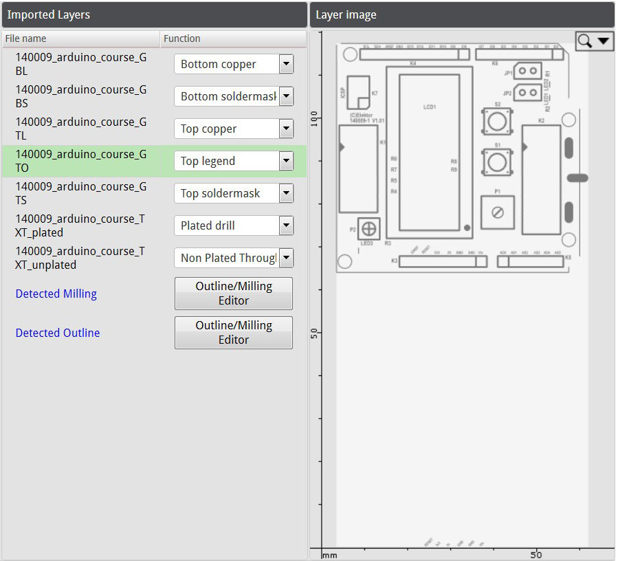
Missing contour segments or open connections can prevent the outline from being correctly interpreted during manufacturing.
Why DRC does not always detect the problem
Design Rule Checks (DRCs) are generally reliable; however, they are not always fully dependable for verifying mechanical geometry. Very small discontinuities or conflicting definitions may go undetected because:
- Gaps are below minimum geometric tolerance thresholds
- Duplicate or conflicting outline definitions exist
- The outline is visually correct but topologically inconsistent
As a result, a final manual inspection remains essential.
“A simple zoomed-in review of the entire outline is often enough to identify issues before release,” explains Saar Drimer in the blog “Let’s talk about outlines”.
As a Hardware designer and technical editor, he highlights that the PCB outline is not just geometry, but the transition from design intent to manufacturable data. He also emphasises that the depanelisation strategy must already be considered when defining the outline.
CAD-to-CAM validation
At Eurocircuits, checking the board outline is fully integrated into the Visualizer workflow. In line with the principle “right first time for manufacturing”, errors are made visible before production starts.
Where necessary, issues are flagged for manual correction. The Outline Editor enables direct fixes within the same workflow:
- Repair of broken or open contours
- Adjustment of misaligned segments
- Cleaning or simplification of geometry
- Verification of copper-to-edge clearances
All changes are immediately re-evaluated for manufacturability.
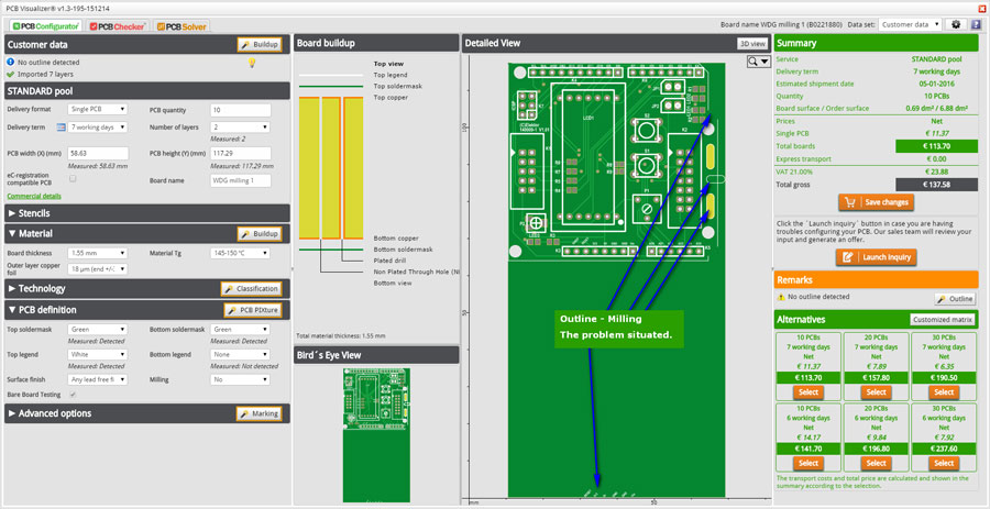
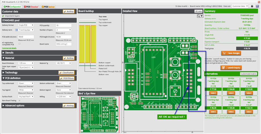
Conclusion
The PCB outline is often treated as a simple drawing task, but it is one of the most critical transition points between CAD intent and CAM execution. Small geometric inconsistencies can still block reliable manufacturing even when all electrical design rules are fulfilled.

Bring your product to market on time and within budget – join the Eurocircuits Community


