What is Soldermask (SM)?
Soldermask is a protective layer of liquid photo image able lacquer applied on the top and bottom side of a Printed Circuit Board. The function of the Soldermask is to protect the copper, apart from the solder pads, from:
- Oxidation
- Creating shorts during
- Soldering (bridges)
- Operation due to external conductive influences
- Operation from net to net due to high Voltage spikes
- Environmental influences like dust and other contaminations that may create shorts in the long run
The Soldermask is first printed or sprayed on to the production panel and then UV-exposed with the correct solder mask pattern, developed and dried. Soldermask is usually green but can also be applied as: black, blue, white, red, clear, etc… Look here to see how it is done in production.
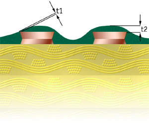
Thickness:
On conductor side edges : > 7 micron (t1).
On conductor top : > 7 micron (t2).
Maximum Soldermask thickness can be up to 40µm for 35µm finished copper thickness. For higher final copper thicknesses, the Soldermask thickness can be up to 80µm
Solder Mask Registrations: what we allow and what not
- The Soldermask may encroach on lands as long as the minimum annular ring requirements are maintained.
- Soldermask is permitted in those PTH not intended for solder fill.
- No isolated pads are exposed.
- No Soldermask encroachment on edge board connector fingers or test points.
- On SMT-pads with pitch 1,25 mm encroachment is permitted on one side of land only and does not
exceed 50 micron (2 mil). - On SMT-pad with pitch < 1,25 mm encroachment is permitted on one side of land only and does not
exceed 25 micron (1 mil).
Please also see:


