User Guides
Our User Guides provide step-by-step instructions on how to use our free online smart tools and other available software.
The purpose of Soldermask (SM) is to provide a protective coating on the PCB against contamination, oxidisation, humidity, mechanical damage and electrical shorts.
The application of SM requires certain criteria to ensure that it has good adhesion, quality and reliability and the PCB layout has a major influence on this.
The data output from a CAD system for SM is usually negative, this means that only the SM openings are output (usually as pads).
This format of output was inherited from the days before laser plotters or Direct Imaging (DI).

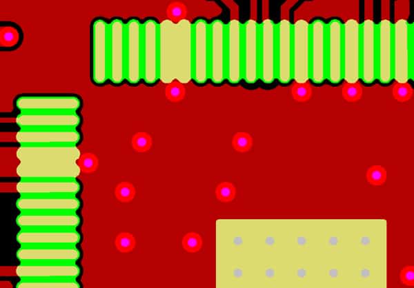
Copper Layer
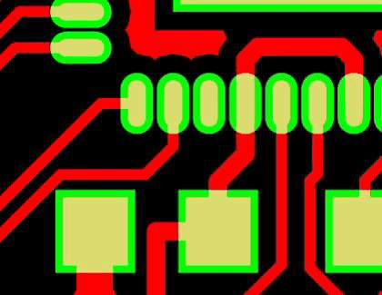
Green is the Soldermask Opening Layer Overlay
As the SM opening is usually larger than the copper pads it is advisable to consider the following points during the layout of the PCB.
The values below are the minimum we require to achieve a good and reliable SM application. These are based on our production parameters and the SM specification. The method of exposure used is defined by the SM colour. The minimum SM opening is 0.40mm
Colours available – Green, Black, Red and Blue. Advantages
LDISoldermaskColour |
Minimum |
|||
MAR |
MSM |
MOC |
||
Green |
0.030mm | 0.075mm | 0.060mm | 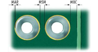 |
Black |
0.030mm | 0.075mm | 0.060mm | |
Red |
0.030mm | 0.075mm | 0.060mm | |
Blue |
0.030mm | 0.075mm | 0.060mm | |
* Soldermask opening shave = 0.005mm Maximum. MAR (Mask Annular Ring) – The clearance from the edge of SM to the edge of the copper pad. MSM (Mask SegMent) – The bridge/web of SM between adjacent pads. MOC (Mask Overlap Clearance) – Distance between a copper track/plane and an adjacent SM opening.
The table below shows the minimum Design Rule values to achieve the minimum LDI Soldermask values.
LDISoldermaskColour |
Minimum |
|||
PP |
TP |
|||
Green |
0.135mm | 0.090mm |  |
|
Black |
0.135mm | 0.090mm | ||
Red |
0.135mm | 0.090mm | ||
Blue |
0.135mm | 0.090mm | ||
PP (Pad to Pad) – The isolation between adjacent copper pads. TP (Track to Pad) – The isolation between adjacent copper pads and tracks/plans. TT (Track to Track) – The isolation between adjacent copper tracks/plans.
Colours available – White or Transparent. Advantages
Photo ImageableSoldermaskColour |
Minimum |
|||
MAR |
MSM |
MOC |
||
White |
0.100mm | 0.130mm | 0.090mm | |
Transparent |
0.100mm | 0.130mm | 0.090mm | |
** Soldermask opening shave = 0.040mm Maximum. MAR (Mask Annular Ring) – The clearance from the edge of SM to the edge of the copper pad. MSM (Mask SegMent) – The bridge/web of SM between adjacent pads. MOC (Mask Overlap Clearance) – Distance between a copper track/plane and an adjacent SM opening.
The table below shows the minimum Design Rule values to achieve the minimum PI Soldermask values.
Photo ImageableSoldermaskColour |
Minimum |
|||
PP |
TP |
|||
White |
0.330mm | 0.190mm | 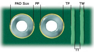 |
|
Transparent |
0.330mm | 0.190mm | ||
PP (Pad to Pad) – The isolation between adjacent copper pads. TP (Track to Pad) – The isolation between adjacent copper pads and tracks/plans. TT (Track to Track) – The isolation between adjacent copper tracks/plans.
Soldermask segments less than he minimum MSM value will be removed as in the example below.
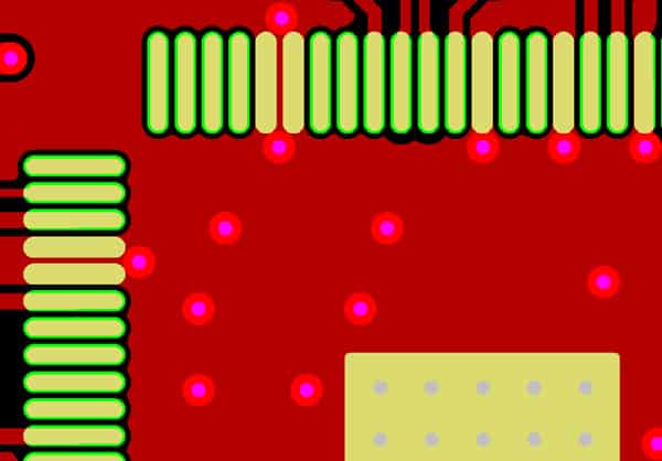
Original CAD Data
MSM less than Minimum Value
This where the copper pad and hole of the Via is to be covered with SM. This is ONLY possible in conjunction with Via Filling.
The reason is that we use a spray coating process to apply SM as this allows for a thinner and more uniform coating. Due to this process and the viscosity of the SM ink it is not suitable for tented via’s as there will always be a small opening on the via hole.
Also, there will be SM ink inside the via barrel and residue may remain after exposure and curing of the SM. This can lead to numerous issue such as bad SM adhesion around the holes or if this residue becomes lose it can cause a bad final finish plating of the component pads due to chemical fluid entrapment etc.
To avoid to these potential issues, we always open all holes (NPTH, PTH and Via Holes) to be free of SM.
In case a hole has no defined Soldermask opening we will define one to be equal to the TOOSIZE used to drill the hole.
Unless Via Filling is selected and the Via’s have no SM opening.
If you require the Via Holes to be closed/covered with SM please select Via Filling with Resin in the Advance options of the PCB Configurator.
In addition, please make sure that you generate your SM data without SM pads/openings for the Via Holes.
NPTH with copper pads should follow the same rules as for Plated Holes. NPTH without a copper pad will requires a Mask Annular Ring (MAR) of 0.125mm.
Always include the board outline in your SM data, this best done using a small line – e.g. 0.50mm wide. The centre of the line should be exactly on the actual board outline (we will remove the line from the final production data).
If you require board edge areas of your PCB to be free of SM, use a wide line to indicate the board outline. The line-width should be at least 2.00mm resulting in 1.00mm border free of SM. It is also advisable to indicate that you require a border free of SM in the mechanical data.
25/06/2020 – DI Soldermask MSM (0.070 to 0.075mm) and PP (0.130 to 0.135mm) values Updated. 13/08/2020 – Tented Via Holes – Explanation updated. 26/10/2020 – Minimum SM opening added.