User Guides
Our User Guides provide step-by-step instructions on how to use our free online smart tools and other available software.
Carbon contacts or patterns are printed with a conductive carbon ink and can be used for keyboard contacts, LCD contacts, jumpers, etc…
Always clearly indicate on which side of the PCB carbon is to be applied, this can be on one side or on both sides.
When generating output please include the board outline.
This is best drawn using a small line – e.g. 0.500mm (20mil) wide where the center of the line is the exact board outline.
We will remove this line from the production data we use to manufacture your boards.
Please indicate the position using proper file names and a clear buildup or layer sequence description in the mechanical layer.
See PCB Design Guidelines – Input Data Requirements and Mechanical Layer pages.
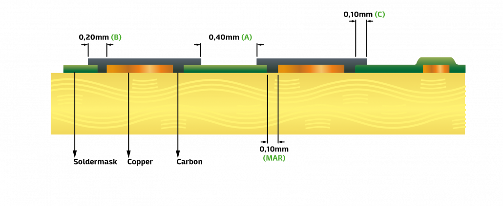 Minimum carbon to carbon spacing (A): 0.400mm (16mil)
Minimum carbon line width: 0.300mm (12mil)
Minimum carbon on copper overlap (B): 0.200mm (8mil)
Minimum carbon on Soldermask overlap (C): 0.100mm (4mil)
These rules mean that you must have a minimal isolation or spacing of 0.800mm (16mil) between the copper elements of a typical carbon finger contact.
 |
 |
 |
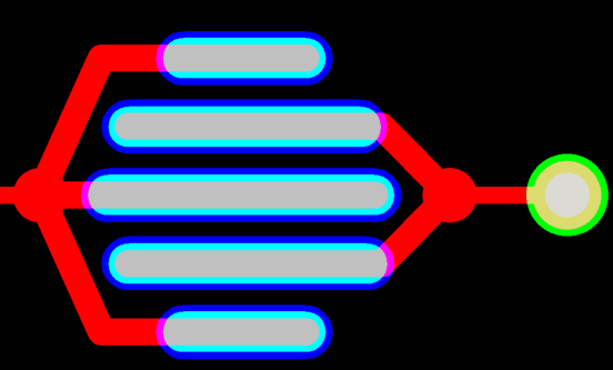
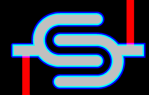
RED = Copper
GREEN/LIGHT BLUE = Soldermask opening
DARK BLUE = Carbon
Please also see our Carbon-Conductive Ink Technical Data Sheets.