User Guides
Our User Guides provide step-by-step instructions on how to use our free online smart tools and other available software.
We refer to Copper Layers as a layer of a PCB that has copper on it after etching, usually tracks and pads or power and ground layers.
When generating output data files use “flashes” for pads and avoid “painted/drawn” pads.
For larger copper areas or copper planes avoid filling them with small draws (“painting”).
Where possible, use contours or polygons to construct areas or planes, these are standard features in Gerber X2 output as well as other data formats.
Always include the board outline when you output your copper layers as this helps us to identify any data alignment, rotation or mirroring issues.
This is best done using a small line – e.g. 0.50mm (20mil) wide – where the centre of the line is the exact board outline.
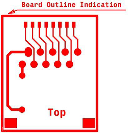
We will remove this line from the production data we produce for the manufacturing process.
Remove copper pads from NPTH holes if these pads are not used or connected to other copper before generating the output data files.
If you require copper pads on NPTH holes please use a minimum Outer Annular Ring (OAR) of 0.30mm (12mil) as defined in our PCB Design Guidelines – Classification page.
Check your final design for small areas of unconnected copper or narrow copper webs and slivers which can lead to problems in production.

X: Must meet classification criterion for minimum Track Width (TW).
A: Avoid if possible.
B: Preferred design
The minimal clearance between edge of board and pattern is.
For routed boards:
For boards with scoring (V-cut) and IMS PCBs:
If you require a copper area or plane to extend up to the board edge please clearly indicate this in the Mechanical Layer.
Copper up to the board edge should only be used where absolutely necessary due to:
For more information see also ‘Copper and the Board Edge‘.
If you require the board edge or part of it to be plated, then clearly indicate this in the Mechanical Layer.
In addition, were the board edge is to be plate there must be copper placed on the top and bottom layers with a minimum width of 0.5mm from the edge of the board inwards.
This is necessary to enable us to produce the Round Edge Plating in such a way, that the metallisation is physically strong enough to stay attached to the side of the board.
For more information see also ‘Copper and the Board Edge‘.
Any text placed in a copper layer has to comply with the design rules for the given class as defined in our PCB Design Guidelines – Classification page.
All copper text must be correctly readable after etching.
A PCB is always viewed from top to bottom through the PCB.
Therefore, the text on the top layer of your board should be readable and the text on the bottom layer should be non-readable or mirrored.
“Peelables” occur during production and are small/narrow pieces of photo resist enclosed by pads, traces and/or planes.
These may “peel” away during processing and cause short or open circuits.
All copper even within the same net must comply with the design rules for the given class as defined in our PCB Design Guidelines – Classification page.

Please see our section on Edge Connectors.
ALWAYS provide the proper layer sequence for a multilayer board.
The layer sequence can be given in several ways:


It is recommended to REMOVE pads from inner layers that the hole does not connect too.
Ensure that the thermal relief pads are properly defined and comply with the chosen pattern classification for Annular Rings (AR), Track Widths (Thermal Segment Width) and Gaps.


A good practice for Thermals is to work with a Gap of 0.20mm (8mil) and a Thermal Segment Width of 0.20mm (8mil).
Use full copper rather than hatching patterns in copper planes.
If you need a hatching pattern, then use following minimum settings:
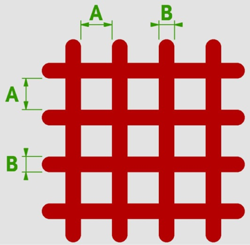
Any hatching pattern that DOES NOT meet these minimum requirements will be converted into a full copper plane.