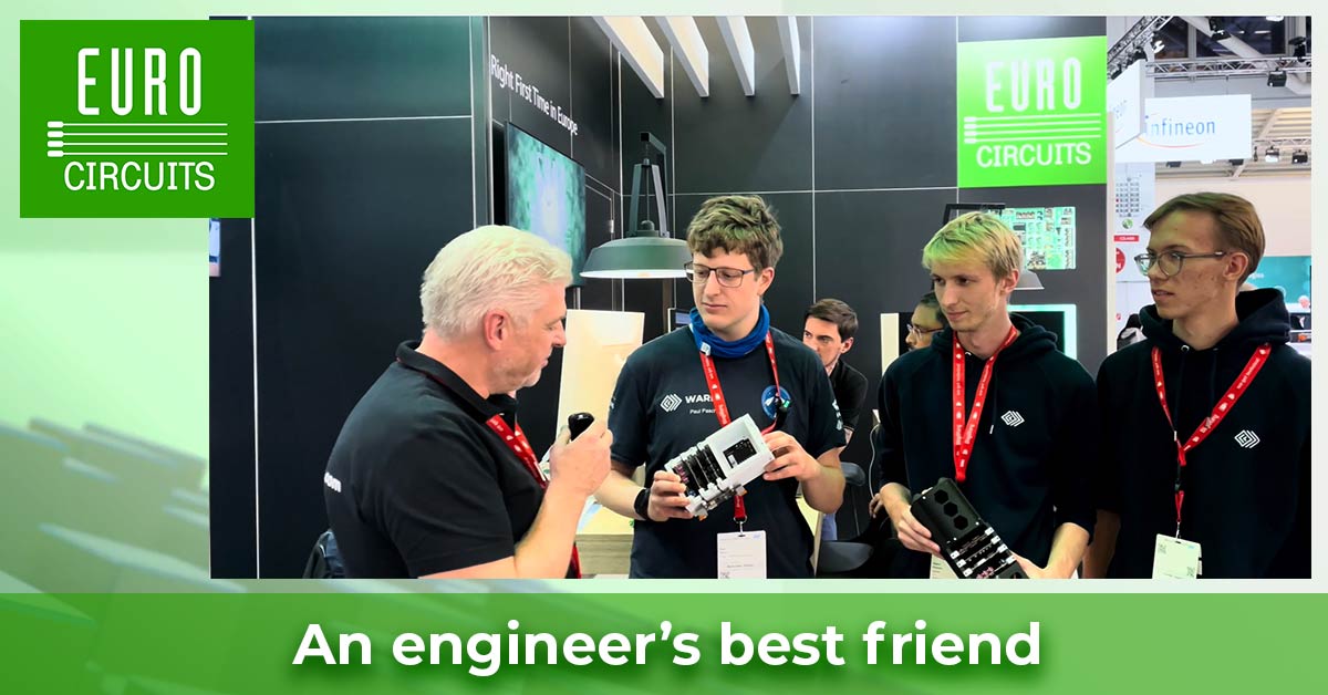
An engineer’s best friend
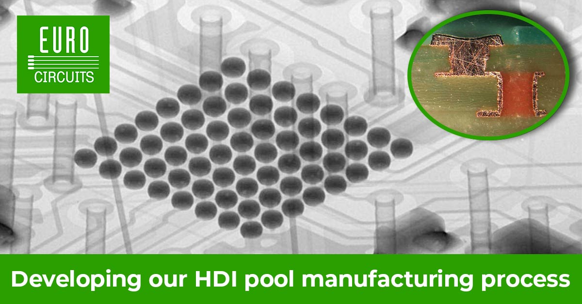
The last three months have been an exciting time for us: full of great conversations, inspiring discussions and valuable contacts at eight fairs and exhibitions across Europe. Each event had its own distinctive character and showcased the passion and innovative spirit of the electronics industry. We presented our new HDI pool at the expos – […]