User Guides
Our User Guides provide step-by-step instructions on how to use our free online smart tools and other available software.
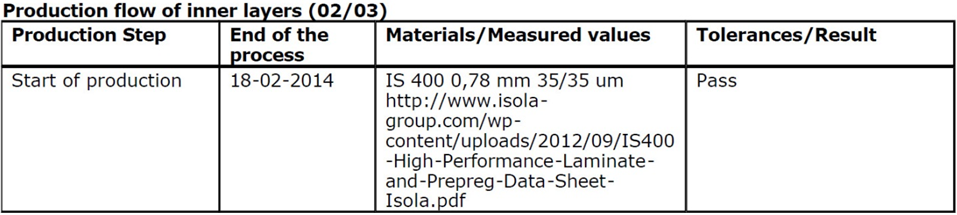
The first step is to make sure that the data that we will use to make your PCBs is correct. To find out how we do this, go to our blog “Front-end Data Preparation“.
We run 3 types of test during fabrication, visual, non-destructive measurements and destructive tests. The destructive tests are used to check our processes. They are made on actual PCBs or on the test coupons which we put onto every production panel. After more than 30 years of PCB manufacturing experience, we have developed test coupons on the production panels which provide simple, non-destructive tests for more complex parameters.
Each fabrication step can be seen in our video “How to Make a PCB”. The sequence below is based on a multilayer PCB. Single- and double-sided boards do not use all these steps, but are tested in the same way.
The results of these checks are summarised for each job in its Passport which contains information on the materials used, measurements made and tests passed. You can access the Passport via the blue book icon with each job under View Running Orders once it has been inspected or under Order repeats/View history.
If you need more information on a job, we have full traceability back to material batches etc. Contact euro@eurocircuits.com or your local sales channel for this service.
We inspect all boards to IPC-A-600 Class 2 This is the standard used for most PCBs, and is the standard most often specified by our customers. The IPC, or Institute for Printed Circuit Boards, is “a global trade association representing all facets of the industry including design, printed circuit board manufacturing and electronics assembly.”
The IPC-A-600 standard “describes the preferred, acceptable and non-conforming conditions that are either externally or internally observable on printed boards”. It divides PCBs into 3 product classes.
Class 2 includes “products where continued performance and extended life is required, and for which uninterrupted service is desired but not critical.” Class 3 (where uninterrupted service is critical) is used for aerospace, defence and medical applications. For more information visit the IPC website.
Customers, especially those supplying the US market, may also specify UL marking. In this case, we further inspect to UL796. The Underwriters’ Laboratory (UL) is “an independent global safety science company …. dedicated to promoting safe living and working environments, UL helps safeguard people, products and places in important ways, facilitating trade and providing peace of mind.”
For PCBs, the most important criterion highlighted by UL marking is flammability. All our FR4 material meets UL 94 V0 plastics flammability test. For more information please see our page What about UL.
This is automatically checked against the order details using a data-matrix. The material data (type, manufacturer, laminate and copper foil thickness) is entered into the job history and will appear in the final Passport.

Visual checks.
This step includes 3 visual checks:
Each production panel has a specially developed test coupon which indicates that the board has been correctly etched and that the track widths and isolation distances are correct. The type of etch resist used and the values for track width, isolation distances and annular ring are entered into the Passport file.
For more information please see our page “PCB Manufacture Step-by-Step“.
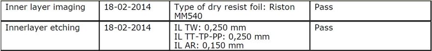
We use Automatic Optical Inspection equipment to scan the inner layer copper and compare it to the design data. The machine checks that all track widths and isolation distances correspond to the design values and that there are no short or open circuits which will cause the finished board to malfunction.
A Pass is entered into the Passport.
![]()
For more information please see our page “Registration and Inspection of Inner Layers in PCB Production“.
Material.
This is automatically checked against the order details using a data-matrix. The material data (type, manufacturer, pre-preg and copper foil) is entered into the job history and will appear in the final Passport.
Thickness after bonding.
This is measured on each production panel and the result entered into the Passport.
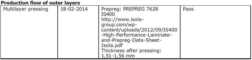
For more information please see our page “PCB Multi-layer Fabrication“.
The drilling machines automatically check drill diameters to ensure that the size of the holes will be correct. A special test coupon on multilayer boards confirms the position of the drilled holes relative to the (already printed) inner layers.
The smallest finished hole size is entered into the Passport.
![]()
For more information please see our page “Drilling Printed Circuit Boards“.
We deposit a layer of carbon on the walls of the holes to make them conductive for electroplating. We enter the process into the Passport.
![]()
Visual checks.
After printing and stripping to make sure that the unwanted plating resist has been stripped away cleanly
Type of resist is entered into the Passport.
![]()

For more information please see our page “Image the Outer Layers“.
Non-destructive sample check.
The operator measures the copper thickness in the holes at 5 or more locations on one panel from every flight bar. The result is entered into the Passport.
![]()

For more information please see our page “Plating“.
Visual checks.
After etching to make sure that all the unwanted copper has been etched away.
Sample check.
Each production panel has a specially developed test coupon which indicates that the board has been correctly etched and that the track widths and isolation distances are correct. The type of etch resist used and the values for track width, isolation distances and annular ring are entered into the Passport file.


For more information please see our page “Etch Outer Layers“.
During process.
Visual checks:
The operator uses a projection microscope to check every panel to ensure that the soldermask is correctly aligned and that there are no solder-mask traces on pads.

The adhesion of the soldermask to the surface of the PCB is checked by the tape test used after legend printing.
The type of soldermask ink used is entered into the Passport data.
![]()
For more information please see our page “Applying Soldermask“.
Sample checks on all surface finishes:
The thickness is measured using an X-ray scope.
We check the adhesion of the surface finish to the surface of the PCB using the tape-test after legend-printing.
100% visual inspection.
The surface must be flat and even across the PCB without any non wetting. Component holes must not be narrowed or blocked. A few via holes may be blocked if they are not covered by soldermask.
The finish must cover all exposed copper and have the same colour across the PCB. There must be no discolouration even in the holes
There must be no tarnishing or blackening.
The surface finish used is entered into the Passport, even where the order is for “Any leadfree”.
![]()
For gold and silver finishes we also enter the actual values measured.

For more information please see our page “RoHS Compliant Surface Finishes“.
Sample checks after curing:
The operator makes a tape test to check the adhesion of the surface finish, soldermask and legend to the surface of the PCB. We press a strip of pressure-sensitive tape across the test area and then pull it off sharply. There should be no bits of copper, surface coating, soldermask or legend ink adhering to the tape.
Visual check.
The operator checks that the legend on every board is clean and legible without blurring or smudging.
For more information please see our page “Silk-Screen and Cure“.
All boards are electrically tested except single-sided boards where electrical testing is an option.
![]()
For more information please see our page “Electrical Test“.
We check the size and position of the board profile and internal milling using special test coupons.
![]()
