User Guides
Our User Guides provide step-by-step instructions on how to use our free online smart tools and other available software.
Eurocircuits are a European manufacturer of standard technology printed circuit boards (or PCBs). Our headquarters are in the picturesque Belgian town of Mechelen and our production units are near Aachen in Germany and at Eger in Hungary. We specialise in providing prototype and small batch PCBs for designers, product development departments, niche market electronics companies, universities and research establishments
The board designer has prepared his layout on a Computer Aided Design or CAD system. Each CAD system uses its own internal data format, so the PCB industry has developed a standard output format to transfer the layout data to the manufacturer. This is Extended Gerber or RS274X. The Gerber files define the copper tracking layers (4 in the job we are following) as well as the soldermasks and component notations…
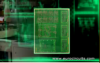
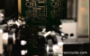
We use laser photoplotters in a temperature and humidity-controlled darkroom to make the films we will use later to image the PCBs. The photoplotter takes the board data and converts it into a pixel image. A laser writes this onto the film. The exposed film is automatically developed and unloaded for the operator.
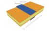
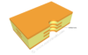
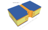
To produce the inner layers of our multilayer PCB, we start with a panel of laminate. Laminate is an epoxy resin and glass-fibre core with copper foil pre-bonded onto each side.
We remove the unwanted copper using a powerful alkaline solution to dissolve (or etch away) the exposed copper. The process is carefully controlled to ensure that the finished conductor widths are exactly as designed. But designers should be aware that thicker copper foils need wider spaces between the tracks. The operator checks carefully that all the unwanted copper has been etched away.
The inner core of our multilayer is now complete. Next we punch the registration holes we will use to align the inner layers to the outer layers. The operator loads the core into the optical punch which lines up the registration targets in the copper pattern and punches the registration holes.
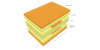
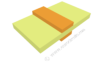
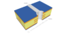
The outer layers of our multilayer consist of sheets of glass cloth pre-impregnated with uncured epoxy resin (prepreg) and a thin copper foil.
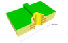
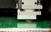
Now we drill the holes for leaded components and the via holes that link the copper layers together. First we use an X-ray drill to locate targets in the copper of the inner layers. The machine drills registration holes to ensure that we will drill precisely through the centre of the inner layer pads.

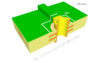
The first step in the plating process is the black hole process, this deposits a thin layer of conductive carbon (nanometres) on the barrel of the holes (only those defined as PTH).
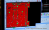
We image the outer layers in a clean room to make sure that no dust gets onto the panel surface where it could cause a short or open circuit on the finished PCB.
Next we electroplate the boards with copper. The operator loads the panels onto the flight bars. He checks all the clamps to ensure a good electrical connection.

We have now plated the panel with 25 microns of copper through the hole and an additional 25 – 30 microns on the tracks and pads. The copper is covered with a thin layer of tin as an etch resist. Now we will remove the unwanted copper foil from the surface.

Most boards have a epoxy-ink soldermask printed onto each side to protect the copper surface and prevent solder shorting between components during assembly.
The copper component pads and holes have been left clear of soldermask. Now we apply a solderable surface finish to protect the copper until the components are soldered onto the board.

For edge-connectors we electroplate hard gold. First the operator puts protective tape on the board above the connectors. Then he mounts the panel on a horizontal electroplating bath.
Most PCBs have a component legend to show which component goes where. Today we use ink-jet printers to image the legends direct from the board digital data.
We electrically test every multilayer PCB against the original board data. Using a flying probe tester we check each net to ensure that it is complete (no open circuits) and does not short to any other net.
The final manufacturing stage is to profile the PCBs and cut them out of the production panel.
Alternatively we can profile the individual circuits on a V-cut or scoring machine. This has two cutters, one above and one below the panel. Each cuts a v-shaped groove about 1/3 of the thickness of the material, leaving a thin web holding the PCBs together.
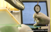
In the last step of the process a team of sharp-eyed inspectors give each PCB a final careful check-over.