Designer Insight: High pin density with smart BGA optimisation
#2 High pin density without HDI smart BGA optimisation
👤 About the Author
Frank R., CID + FED-Designer
📍 Germany
🎯 Specialist in high-density FPGA layouts
“Sometimes the best HDI strategy is not using HDI at all.”
📦 Project Snapshot
FPGA module for video signals
📏 Limited installation space
🔄 Replacement board
💰 Goal: cost-efficient, production-ready solution
⚙️ Technical Challenge
💡 Situation:
At the time of prototyping, partial HDI pool production was not yet available.
The objective:
- Use standard PCB technology
- Keep costs low
- Still achieve high pin density
Classic trade-off: density vs. cost vs. manufacturability
🧩 Engineering Workaround
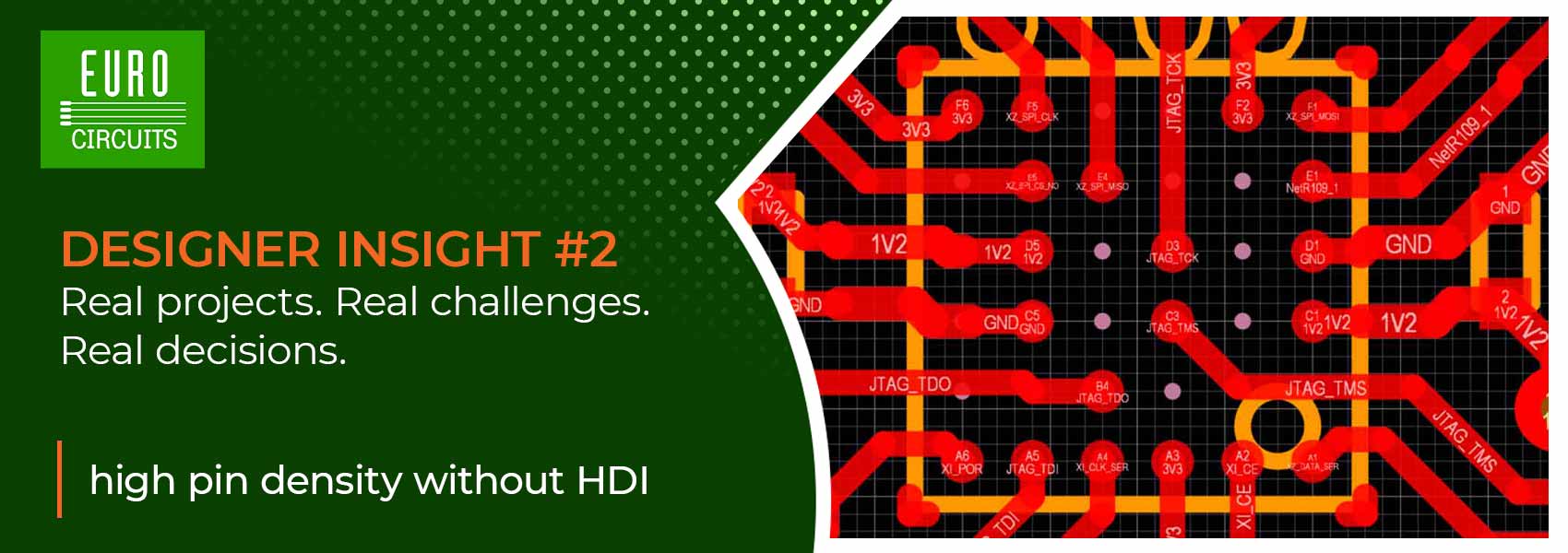
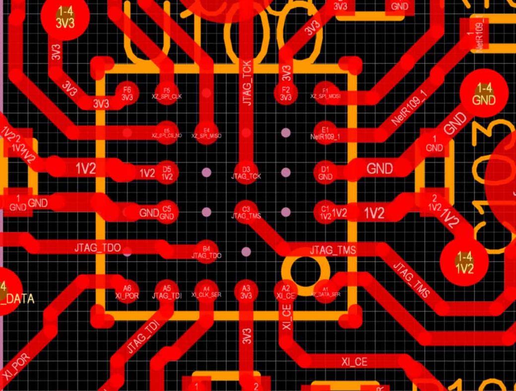
🔬 Optimising the BGA instead of using HDI
Component used: 0.4 mm pitch BGA, 6×6 (BGA36C40P6X6)
Key design decision:
- Unused pads in the outer rows were intentionally removed
- This opened routing channels on the outer layer
- Inner pads became accessible without HDI
Result: High connection density achieved with a standard 4-layer buildup.
🏭 Eurocircuits Contribution
🚀 4-layer pooled production in standard technology
- Cost-efficient prototypes
- Production-capable solution
- No HDI process required
🔍 Design Review in the PCB Visualizer
- Deviations from the expected footprint were detected
- Reviewed with the designer
- Confirmed as intentional design strategy
👉 No correction needed – but full transparency ensured.
📊 Result & Benefit
✅ Production-ready solution
✅ Fast prototype turnaround
✅ Cost-efficient implementation
✅ High pin density without HDI
💬 Designer’s Opinion
“The Eurocircuits HDI pool solution was not yet available at the time. Therefore, a manufacturable solution using standard technology was developed.”
🔎 What Other Designers Can Learn
💡 HDI is not always required
💡 Component strategy can replace process complexity
💡 Removing unused pads can unlock routing space
💡 Design reviews validate even unconventional approaches
Bring your product to market on time and within budget – join the Eurocircuits Community


![]()

