The Materials section offers various options to configure the build of your PCB, the available options vary depending upon which Service you have selected.
IMPORTANT
- The defaults offer the best cost efficiency.
- Selecting alternative materials may affect the price and lead time.

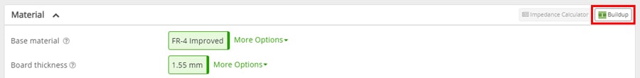
You may also open the Buildup Editor to define and visualise the buildup of your PCB, simply click on the Buildup Editor button in the top righthand corn of the section.
If you have selected the DEFINED IMPEDANCE service then you will also be able to open the Impedance Calculator which will help you calculate the track, isolation and copper thickness to achieve your required impedance.
To access the Impedance Calculator, make sure you have selected the DEFINED IMPEDANCE service and then click on the Impedance Calculator button in the top righthand corner of the section.

Base material
Select the type of base material to be used for the manufacture of your PCB and depending on which Service you have selected will define the default material and the available additional options.
NOTE
- The defaults offer the best cost efficiency.
- The drop-down menu More options show all the available Base materials and which service they applicable too.
See also:
Base Material Data sheets
Board thickness
The nominal thickness label of your PCB.
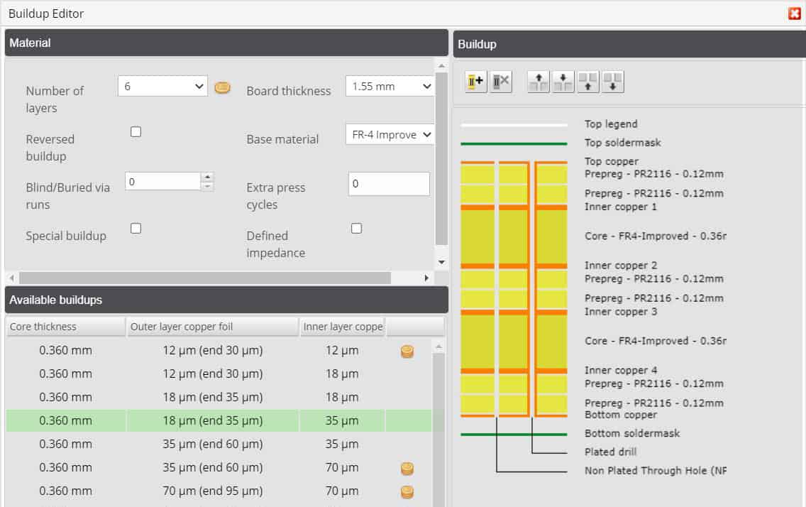
This does not consider the actual materials used in the buildup of your PCB. To have a more accurate calculated thickness you need to open the Buildup Editor.
Here you can see the calculated Total material thickness of the selected buildup and where you can select different or more suitable buildups which may change the calculated Total material thickness.
NOTE
- The defaults offer the best cost efficiency.
- The final thickness of the PCB after manufacturing will be within 10% of the calculated Total material thickness.
See also:
The complex story of PCB thickness
Finished PCB Thickness Tolerance
Material Tg
The Material glass transition temperature (Tg) is the temperature at which the Base material becomes mechanically unstable and is defined by the Base material you select.
When you select a different material then the Tg value may change, if you select a different Tg then the Base material may change.
NOTE
- If multiple material types are used as in the case of RF pool multilayer PCBs then the Material Tg value shown is taken from the material with the lowest Tg.
See also:
What is material Tg
Base Material Data sheets
Outer layer copper foil
Select the nominal start outer layer copper foil thickness to be used in the manufacture of your PCB.
When selecting the start thickness of the copper foil also check that figure in brackets is suitable for your design as this represents the nominal final outer layer copper thickness.

See also:
Tolerances on Copper Thickness
PCB Design Guidelines – Classification
Inner layer copper foil
Only available for PCBs with 4 layers or more.
Select the nominal start inner layer copper foil thickness to be used in the manufacture of your PCB.
This is also the nominal final inner layer copper thickness.

See also:
Tolerances on Copper Thickness
PCB Design Guidelines – Classification
Reverse Buildup
Only available for PCBs with 4 layers or more.
Select this option if you require your multilayer PCB to be manufactured using the Reverse buildup method.
NOTE
- A normal buildup uses cores for the internal layers and prepreg covered in copper foil for the outer layers. Whereas a reversed buildup uses cores for both inner and outer layers with prepreg between the cores, see the images below.
 Standard Buildup
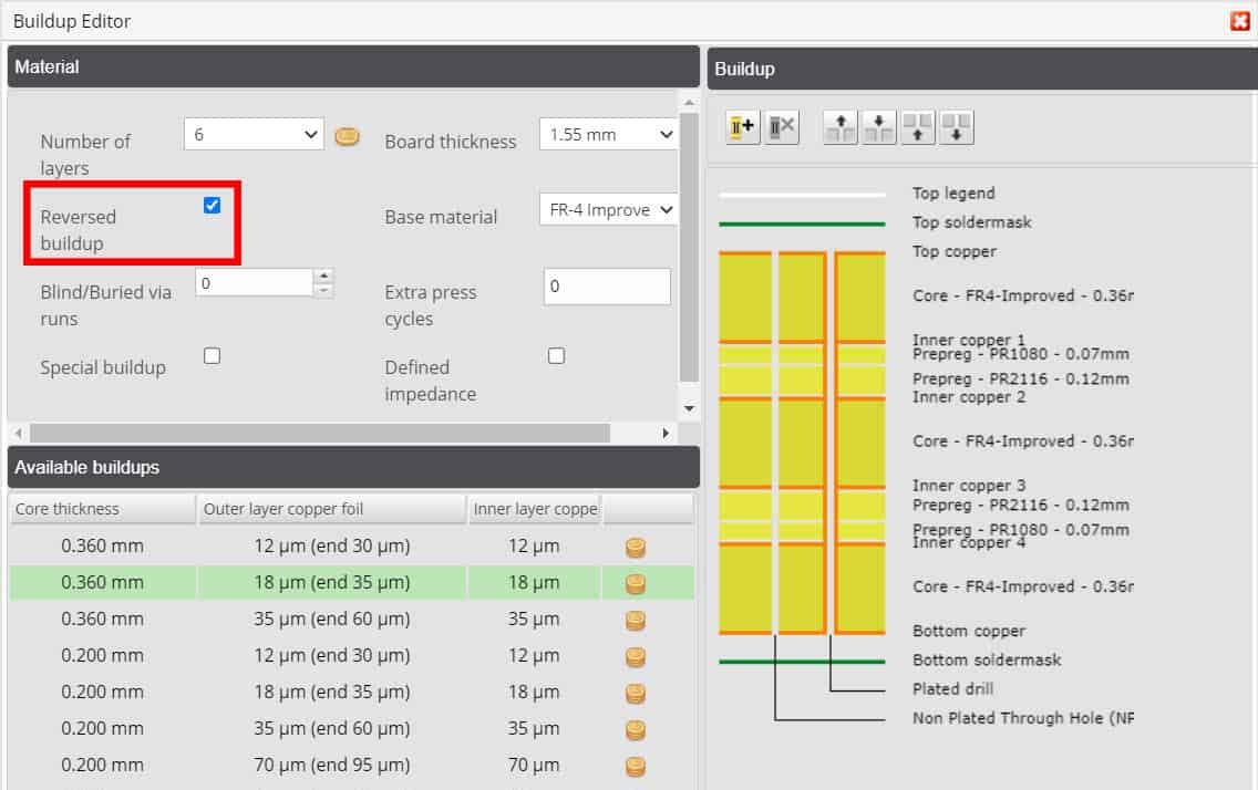 Reverse Buildup
See also:
Buildup Editor
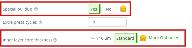
Special buildup
Only available for PCBs with 4 layers or more.
Select this option if you require a buildup that is not available by using one of the predefined buildups.
No online price will be calculated, and our technical team will work out a proposal.
Extra press cycles
Only available for PCBs with 4 layers or more.
Input the number of Extra press cycle required for designs that use Blind and/or Buried vias.
NOTE
- The number of extra press cycles will increase the price of your PCB(s).
See also:
What is an extra press cycle?
Inner layer core thickness
Default – Standard
Only available for PCBs with 4 layers or more and if Special buildup is selected.
Select an alternative from the list of available thickness and those in the drop-down More options list.
See also:
What is the core of a PCB?
Blind/Buried via runs
Only available for PCBs with 4 layers or more.
Input the number of Blind/Buried via runs required for the manufacture of your PCB.
For producing Blind and/or Buried holes we use the sequential buildup method.
Depending on the type of buildup may require more than one standard through hole plating cycle.
NOTE
- The number of Blind/Buried via runs will increase the price of your PCB(s).
See also:
What is an extra PTH run?