The Technology section provides options for selecting the technology of your PCB which will then determine the Technology class of your PCB design.

Full Analysis
If you upload data with full analysis, then the default values will be selected based on the layers defined in your data.
These values will also set the Technology class of your PCB and therefore have an impact on the price of the PCB(s)
The minimum measured value for each parameter found will be displayed in each row as in the example in the image below.

All these parameters can be changed to suit your requirements.
If the Measured value is a + sign, then it means that the size of value of the parameter measured is larger than available options but is still ok for manufacture.
NOTE
- If you change any of the values to be larger than the measured value a warning message will appear as in the example below.

The message also provides you with 3 options:
- Accept – This will revert the value to the original value set by the Full Analysis.
- Ignore – This will keep value that you have defined.
- PCB Checker – This will open the PCB Checker where you can check which value is correct.
Basic Analysis
If you run only basic analysis on your data, then these parameters will need to be updated manually as necessary to match the minimum values of your PCB.
These values will also set the Technology class of your PCB and therefore have an impact on the price of the PCB(s).
No Data
If you do not upload any data, then these parameters will need to be updated manually as necessary to match the minimum values of your PCB.
These values will also set the Technology class of your PCB and therefore have an impact on the price of the PCB(s).
Classification
In the Technology section there is the Classification button.
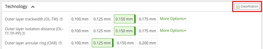
If you click on this, it will open the Classification editor in a popup window as below with the current selected values set in the Technology section.
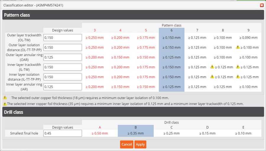
The table displayed in the popup window is dynamic table that is automatically updated based on the parameters defined in the PCB Configurator.
Using this table, you can select the Pattern and Drill class of your PCB design.
Simply click on the column that contains the appropriate values (the column will turn blue) and then select apply.
This will update the applicable values in the Technology section and the Technology class.
Remarks may be displayed together with the  symbol next to the value in the table based on the values set or select to provide additional information and guidance.

Outer layer track width (OL-TW)
Default – 0.150mm
The minimum track width on the outer layers of the PCB.
See also:
What is Track Width
Track Width and Isolation Gap Tolerances
Technical Terms and Abbreviations
Outer layer isolation distance (OL-TT-TP-PP)
Default – 0.150mm
Minimum isolation distance between any 2 copper features (track to track, track to pad, pad to pad) on the outer layer of your PCB.
See also:
What is Track to Track (TT)
Track Width and Isolation Gap Tolerances
Technical Terms and Abbreviations
Outer layer annular ring (OAR)
Default – 0.125mm
The minimum outer layer annular ring, this is the edge of the drilled hole to the outer edge of the copper pad.
See also:
What is Outer Annular Ring (OAR)
Technical Terms and Abbreviations
PCB Design Guidelines – Classification
Understanding Annular Rings
Inner layer track (IL-TW)
Only available for PCBs with 4 layers or more.
Default – 0.150mm
The minimum track width on the inner layers of the PCB.
See also:
What is Track Width
Track Width and Isolation Gap Tolerances
Technical Terms and Abbreviations
Inner layer isolation distance (IL-TT-TP-PP)
Only available for PCBs with 4 layers or more.
Default – 0.150mm
Minimum isolation distance between any 2 copper features (track to track, track to pad, pad to pad) on the inner layers of the PCB.
See also:
What is Track to Track (TT)
Track Width and Isolation Gap Tolerances
Technical Terms and Abbreviations
Inner layer annular ring (IAR)
Only available for PCBs with 4 layers or more.
Default – 0.125mm
The minimum inner layer annular ring, this is the edge of the drilled hole to the outer edge of the copper pad.
See also:
What is Inner Annular Ring (IAR)
Technical Terms and Abbreviations
PCB Design Guidelines – Classification
Understanding Annular Rings
Smallest final hole
Default – 0.45mm
The smallest final drilled hole diameter on the PCB (plated or non-plated).
See also:
PCB Design Guidelines – Drilled Holes
Holes <= may be reduced
Default – 0.45mm
Final holes sizes smaller or equal to this given diameter are by DEFAULT defined as Via Holes and may be reduced to allow for the correct annular ring values.
See also:
Technical Terms and Abbreviations
Hole density
Default – < 1000/dm2
The number of holes per square decimetre.
Normal standard technology boards on average have in average less than 1.000 holes / dm², higher hole density will increase the drilling time and thus the price.
Component pad pitch
Default – 0.50mm
The smallest pitch between to pads of the same component.
Technology class
Technical classification for the layout pattern and drill holes based on the values input or measured during Full analysis.
This value non-editable and is automatically updated when the values in the Technology section are changed.
See also:
PCB Design Guidelines – Classification