User Guides
Our User Guides provide step-by-step instructions on how to use our free online smart tools and other available software.
The Track widths and isolation gaps are defined in the DRC parameters of your CAD system in a little as 0.001mm (1µm) steps.
These are taken by manufacturer to be the nominal values and are used to help set the parameters for production.
The values should be based on a “Right First Time Design for Manufacturing” principle and functionality of the PCB.
Track widths and isolation gaps are important as they define the current load, impedance and electronic signal integrity for a PCB.
Therefore, the track widths chosen depend upon the actual functionality of the PCB. For example, high current requires wider traces and isolation gaps as normal signal tacks.
The main factors that influence the final track widths and isolation gaps are listed below:
As a manufacturer we know how to manage and compensate for the factors above.
However, it is not possible to fully compensate for each one and thus tolerances are introduced.
When measuring a track width. you must do so where the copper meets the laminate, not the top of track.
In accordance with the IPC A-600 the acceptable tolerance for track widths and isolation gaps is 20%.
The base copper thickness will define the minimum possible values for the track widths and isolation gaps.
The thicker the copper the wider the minimum track width and isolation gap must be.
The copper thickness is important for the functionality of a PCB, for example, higher current requires thicker copper.
Please see our PCB Design Guidelines – Classification page.
When it comes to imaging of the track patterns there are two possibilities, conventional using photo-tools or Direct Imaging (DI).
DI is the latest technology and is the most accurate method of imaging, it eliminates many of the issues caused by the conventional photo-tool process.
Using a photo-tool may result in light passing through it to be defused, causing the tracks to enlarged or reduced during the imaging process.
The distribution of copper on a layer of a PCB determines the rate at which the copper is removed.
Copper balance is important for the uniformed removal of the unwanted copper during the etching process.
Uneven copper balance will results in the smaller areas of copper etching quicker than large areas.
Etching is a chemical process and relies on the right parameters to provide a balanced and even removal of the unwanted copper.
Based on the class of PCB design and the base copper thickness we know what will happen during the etching process.
We know how long to etch the PCB to have the optimum result and more importantly we know what compensation to add to the track widths to give us the desired finished track widths.
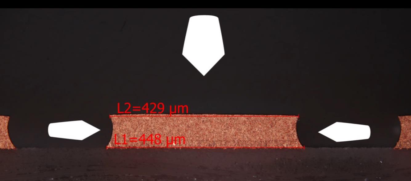
Below is an example of a track after etching, as you can see the bottom (attached to the laminate) is wider than the top.
This is because the etching process is both a downward and sideways process.
Our CAM preparations we apply etch compensation of between 0.001-0.004mm (1-4µm) to copper features (track, pads etc).
This compensates for over etching that we use to ensure all of the copper is removed from the isolation gaps.