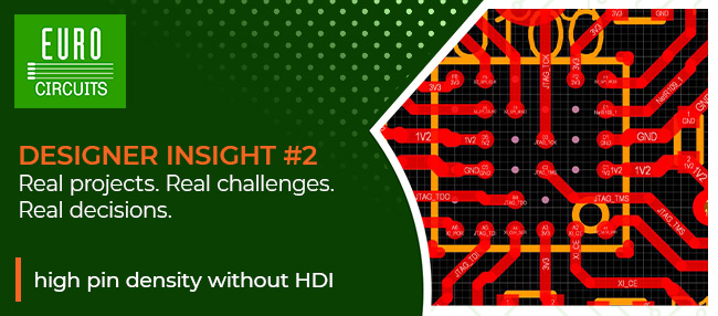
FPGA Routing: High Pin Density without HDI
Designer Insights #2: Real projects. Real challenges. Real decisions.
Does high pin density automatically require HDI? Not necessarily.
In our second Designer Insight, Frank (CID+) shows how a dense FPGA layout was realised using standard PCB technology without HDI processing and without unnecessary manufacturing complexity.
The challenge: limited installation space, high connection density, and the need for a cost-efficient, production-ready solution. At the time, the Eurocircuits Partial HDI pool service was not yet available. So instead of increasing process complexity, the design strategy focused on something else: optimising the BGA itself.
By intentionally removing unused pads in the outer rows of a 0.4 mm pitch BGA, additional routing channels were created on the outer layer. This made the inner pads accessible using a standard 4-layer pooled buildup from Eurocircuits.
During the PCB Visualizer review, deviations from the expected footprint were detected, reviewed together with the designer, and confirmed as an intentional engineering decision.
Result: high pin density, fast prototype turnaround, and a production-capable solution without HDI.
Your experience matters
This is the second part of our Designer Insights series built on real-world challenges and practical engineering decisions.
Have you solved a tricky layout, manufacturing, or data challenge?
Share your insight with the community, anonymously or with your name/company.
Because the best solutions are the ones engineers learn from each other.
Bring your product to market on time and within budget – join the Eurocircuits Community


![]()

