
User Guides
Our User Guides provide step-by-step instructions on how to use our free online smart tools and other available software.
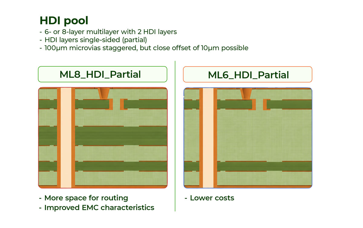
Eurocircuits’ HDI Pool gives electronics designers cost-effective access to microvia technology through standardised 6- and 8-layer PCB build-ups and defined manufacturing parameters.
The construction uses two staggered microvia layers on one side of the PCB, connecting the first three copper layers. Depending on the selected build-up, this microvia structure can be located on either the top or the bottom side of the PCB. The rest of the board retains a more conventional multilayer construction.
Because the HDI structure is limited to one side and the PCB can be manufactured using a single multilayer pressing cycle, this is referred to as partial HDI.
The smaller microvias create more space to route the connections of fine-pitch components than conventional drilled vias. This can make it possible to integrate a component that cannot be routed efficiently using standard multilayer technology, without introducing HDI technology throughout the complete PCB.
HDI Pool therefore provides a practical bridge between conventional multilayer PCBs and complex, fully customised HDI constructions. It is particularly suitable when one or a limited number of fine-pitch components require additional routing space, while the rest of the design can remain comparatively straightforward.
To calculate your HDI pool configuration and download the available Design Rule Files (Altium) click on the button below.
HDI pool provides a defined route from PCB design to verified production:
This enables the engineer to move from a known manufacturing build-up to a pre-production verified design and then into poolable HDI manufacturing.
A single fine-pitch component should not necessarily force the complete PCB into a complex, fully customised HDI manufacturing process.
HDI pool allows microvias to be used in the areas and layers where they are required, while the remainder of the construction stays as straightforward as the application allows.
HDI pool uses defined build-ups, qualified materials and controlled manufacturing parameters. This makes it possible to combine compatible customer orders on shared production panels.
The pooling principle:
Standardised build-ups are manufactured repeatedly using the same qualified materials and controlled process route. This allows production results to be measured, reviewed and continuously refined rather than treating every HDI board as a completely new manufacturing project.
For the engineer, this means a more controlled and repeatable route from verified design data to the finished PCB.
A controlled selection of qualified materials reduces dependence on uncommon materials and one-off constructions. It also helps Eurocircuits concentrate demand on materials that are used repeatedly within the service.
Microvias can make it possible to fan out compact component packages where conventional drilled vias consume too much space.
HDI pool may support BGA pitches down to 0.4 mm, depending on the pad geometry, pin arrangement, pin utilisation, track and clearance requirements, and the component manufacturer’s recommended fan-out.
Microvias use less PCB area than conventional through-vias. They allow signals to move between adjacent layers while preserving routing space for tracks, reference planes and other components.
A conventional through-via can create an unused stub beyond the layers used by the signal. At higher frequencies, the complete via structure can influence reflections and signal integrity. Microvias create shorter transitions between adjacent layers and can support more controlled high-speed interconnect structures when used as part of a properly engineered stack-up and routing strategy.
Shortening the signal transition is only part of the design problem. The return current must also be able to move between the corresponding reference planes through a nearby ground connection. A short microvia transition cannot compensate for an interrupted reference plane or a signal routed across a plane split.
Copper-filled microvias can connect the thermal pad of a QFN or another power-dense component to an internal copper plane. When correctly designed and manufactured, this can support heat transfer while avoiding the soldering risks associated with open through-hole vias inside a component pad.
The HDI pool build-ups provide compact spacing between signal and reference layers. At high frequencies, the return current normally follows the path of lowest impedance on the nearest reference plane, directly beneath the signal trace.
A close and continuous reference plane helps reduce the signal-return loop area and supports a defined impedance structure. Signals should not be routed across gaps or splits in their reference plane, as this forces the return current to take a longer and less predictable path.
A BGA fan-out is not complete simply because every connection can be routed. The layer assignment must also preserve continuous reference planes and controlled return-current paths. Power distribution, ground connections and thermal paths must be considered alongside signal escape and routing density.
Final EMC and signal-integrity performance depends on the complete PCB and product design, not on the build-up alone.
When only part of the design requires microvias, partial HDI can provide the required interconnect functionality without applying advanced technology throughout the complete layer structure.
Eurocircuits and the HDI design experts at CIBOARD electronic developed a practical six-layer demonstration board using real component packages.
Six-layer HDI pool demonstration board showing three partial-HDI applications: 0.5 mm micro-BGA fan-out, 0.4 mm controlled high-speed routing and a QFN thermal-pad connection.
Six-layer HDI pool demonstration board showing three partial-HDI applications: 0.5 mm micro-BGA fan-out, 0.4 mm controlled high-speed routing and a QFN thermal-pad connection.
The board demonstrates how partial HDI technology can solve three different PCB design challenges:
These examples show how advanced interconnect technology can be applied locally, while the remainder of the PCB retains a standardised multilayer construction.
These examples should not be treated merely as routing exercises. Each solution must be evaluated within the complete PCB and PCBA design, including signal and return-current paths, reference-plane continuity, impedance, power distribution, thermal management and assembly.
Developed with the HDI design experts at CIBOARD electronic.
The demonstration board includes a micro-BGA with a 4 × 4 pin arrangement and 0.5 mm pitch.
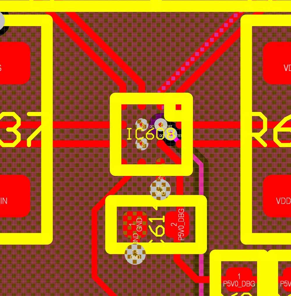
0.5 mm pitch micro-BGA fan-out using L1 and L3 for signal routing, L2 as the ground reference plane and L1–L2 microvias for ground connections. Design and graphic provided by CIBOARD electronic.
The example uses:
The microvias create the additional routing space required around the component without forcing the complete PCB into a fully customised HDI stack-up.
Result: a compact BGA fan-out within a standardised six-layer partial-HDI build-up, with L2 providing a nearby ground reference and L1–L2 microvias supporting the ground connections. Final suitability still depends on the complete signal, power, return-path and thermal design.
The demonstration board also includes a 0.4 mm pitch micro-BGA with differential signal pairs and impedance requirements.
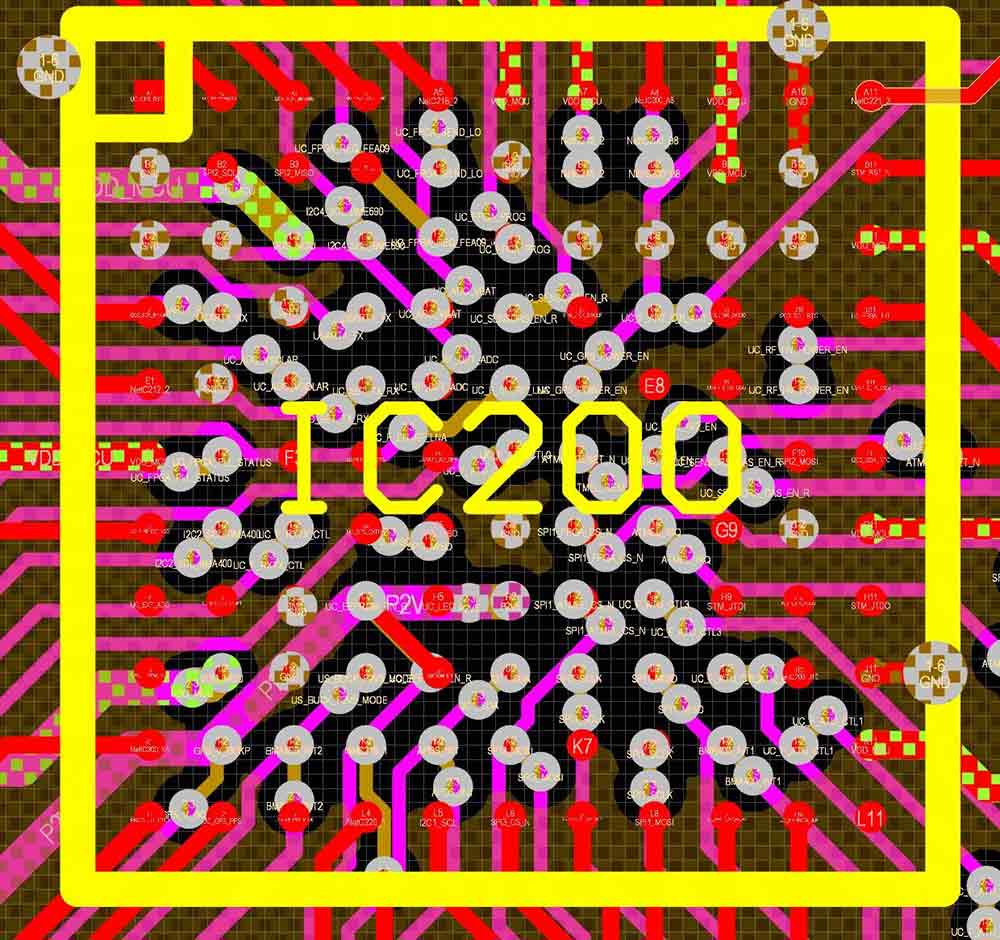
0.4 mm pitch micro-BGA fan-out with defined impedance differential pairs and staggered microvia transitions. Design and graphic provided by CIBOARD electronic.
The example uses:
When a signal changes layers, the designer should consider both the signal transition and the associated return-current path. Where the reference changes between planes, a nearby ground transition can help the return current follow the signal without creating an unnecessarily large loop.
Compared with a conventional through-via transition, the partial-HDI construction avoids an unused through-via stub. This can reduce discontinuities and support more controlled high-speed signal transitions.
A short, stub-free signal transition is beneficial, but it does not compensate for an interrupted reference plane, an uncontrolled return-current transition or inadequate power and thermal design.
Result: a compact, defined impedance fan-out without introducing a fully customised HDI construction.
Design consideration: Keep reference planes continuous, avoid unnecessary layer changes and do not route defined impedance signals across gaps or splits in their reference plane.
The demonstration board uses a QFN48 component with a 0.5 mm pitch. Copper-filled microvias connect the component’s thermal pad directly to the L2 ground plane.
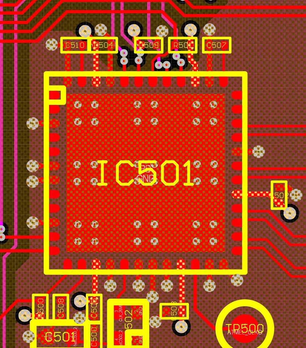
QFN48 thermal pad connected to the L2 ground plane using copper-filled microvias. Design and graphic provided by CIBOARD electronic.
Where additional heat spreading is required, staggered microvias between L2 and L3 can connect the ground plane to a further copper area on L3.
Because the outer microvias are filled and planarised, the component can be soldered over the via area without the solder-loss risks associated with open through-hole vias in the pad.
Result: a controlled thermal connection to internal copper while maintaining a suitable soldering surface beneath the component.
further example: Designer Insight: partial HDI PCB differential signals FPGA routing
Check out your parameters in PCB configurator and download the Design Rule Files (Altium).
HDI pool is intended for PCB designers and electronics development teams that need controlled access to microvia technology for prototypes, NPI and low-volume production.
Typical applications include:
HDI pool can be particularly relevant when:
Not every fine-pitch component automatically requires an HDI PCB. The answer depends on the complete package, fan-out and routing problem, not on component pitch alone.
Important factors include:
In some cases, component selection or a different fan-out strategy may allow the design to remain within standard multilayer technology. In others, microvias may provide the most controlled and economical solution.
Eurocircuits can help evaluate the design before unnecessary complexity becomes embedded in the layout.
HDI pool currently provides a defined manufacturing route for compatible designs, including:
The use of staggered rather than stacked microvias provides a controlled construction that combines useful routing density with a repeatable manufacturing process.
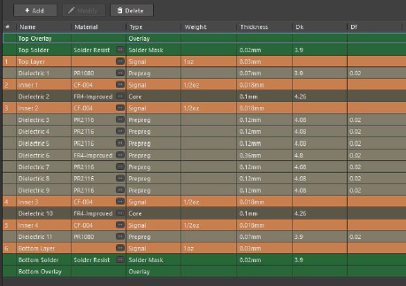
The Altium Design Rule template (.RUL file) and the PCB Buildup (.stackupx file) for your PCB layout are available to download from your Eurocircuits customer account.
Try it now: Upload your design to the Eurocircuits Visualizer, check it online for manufacturability and start your partial HDI PCB right away.
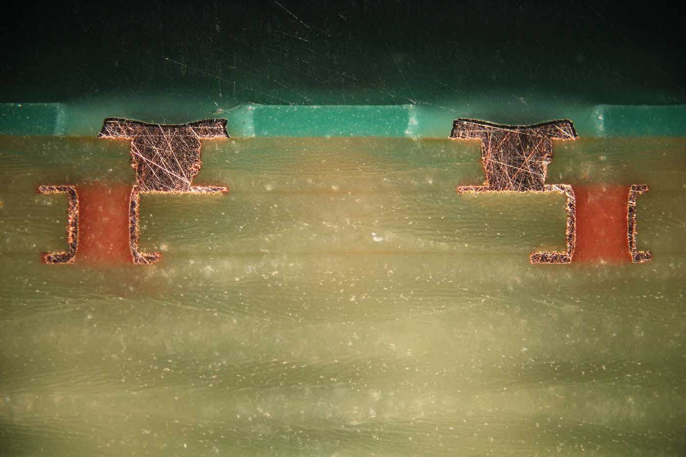
Microsection of 100 µm staggered microvias.
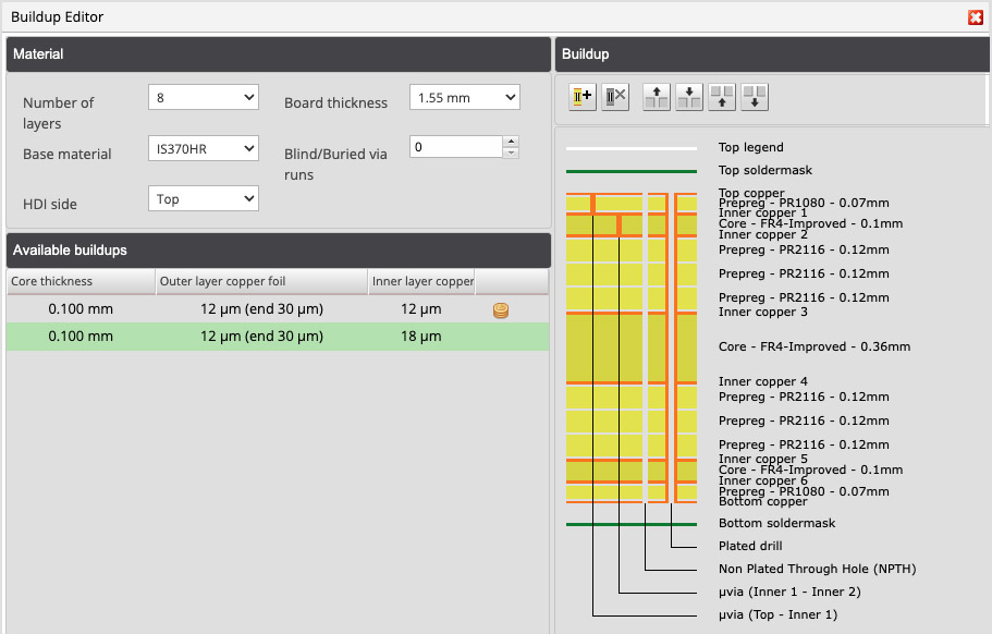
Visualizer Buildup editor
View the complete technical specifications.
Start the PCB design with a known, manufacturable layer structure rather than adapting the completed layout to an available build-up afterwards.
Use the published HDI pool build-up data and CAD design-rule files to configure your design environment with the correct manufacturing parameters from the beginning.
For Altium Designer, Eurocircuits provides an HDI pool Design Rule template in .RUL format and a PCB build-up file in .stackupx format. These files can be downloaded from your Eurocircuits customer account and imported into the PCB design environment.
Starting with the correct build-up and design rules reduces the risk of having to adapt a completed layout to the manufacturing service afterwards.
Define the required characteristic and differential impedances before beginning the detailed routing.
PCB impedance depends on more than track width alone. Relevant factors include:
Use the Eurocircuits impedance tools with the actual HDI pool build-up to determine suitable routing geometries. The calculated values support the design process, but the complete electrical behaviour still depends on the manufacturing tolerances, signal transitions, reference planes and overall routing structure.
Upload the PCB data to the Eurocircuits Visualizer before ordering. The Visualizer virtually manufactures the design and creates a digital twin of the proposed PCB. Automated DRC and DFM analysis then compares the data with the selected HDI pool parameters.
The analysis can identify concerns such as:
When assembly data are supplied, the analysis extends beyond the bare PCB. Depending on the available component data, automated checks can also identify concerns involving:
Together, these analyses provide a holistic view of the PCB and PCBA before production. The automated results support rapid engineering decisions, while Eurocircuits specialists remain available when individual review or more advanced assistance is required.
Automated verification does not replace the engineer’s design responsibility, but it helps expose avoidable manufacturing risks before physical production begins.
When the design and selected options are compatible with HDI pool, the online calculator immediately provides the price and available delivery terms.
HDI pool bare boards are currently available from 12 working days. Complete PCB assembly is available from 17 working days, subject to design compatibility, component availability, order quantity and the selected service options. Available lead times are shown in the calculator.
Eurocircuits can manufacture the HDI PCB, source the components and assemble the complete board. This provides one controlled route from verified design data to an assembled prototype or low-volume production order, reducing the need to coordinate separate PCB and assembly suppliers during the critical prototype and NPI stages.
This holistic view of the PCB and PCBA helps the engineer evaluate manufacturability, assembly feasibility, component availability and cost through one connected process.
It starts with your Design Rule Files for your CAD system, input your PCB parameters in our PCB Calculator and download your CAD DRC files.
Miniaturisation leaves less room for error.
Smaller features and compact component packages require tighter control throughout PCB manufacturing and assembly.
Before the introduction of the HDI pool, Eurocircuits developed and evaluated the manufacturing and assembly process using dedicated test panels and representative fine-pitch components. The validation work included:
The resulting process knowledge was then applied to a practical six-layer demonstration board developed with CIBOARD electronic. The board combines fine-pitch BGA fan-out, defined impedance high-speed routing and QFN thermal-pad connections in one representative design.
This links manufacturing validation to realistic PCB design applications rather than evaluating isolated test structures alone.
This manufacturing knowledge is combined with pre-production verification in the Eurocircuits Visualizer. The objective is to identify detectable and avoidable risks before the design reaches the production floor and to support the manufacture and assembly of the design Right First Time.
Book a personal HDI pool demonstration
Do you have a fine-pitch component, BGA fan-out or HDI design challenge?
Book an online demonstration with a Eurocircuits specialist.
The demonstration is a practical engineering conversation about the design and whether HDI pool is the right solution.
It can cover:
Where appropriate, you can bring a specific design challenge or component package for discussion. This is not a general sales presentation: it is a focused discussion about your design.
Use the following authoritative resources to understand the technology, evaluate whether it suits the application and prepare a manufacturable design.
Review the currently available build-ups, materials, dimensions, design parameters, surface finishes and assembly options.
Learn how to route fine-pitch BGAs using staggered microvias while preserving continuous reference planes, controlled return-current paths and suitable power and thermal connections.
Understand how partial HDI can support BGA fan-out, high-speed interconnect design and thermal management without requiring a fully customised HDI construction.
Understand how component package selection, pad size, track width, clearance and via placement influence manufacturing complexity and price.
See how Eurocircuits developed and evaluated the microvia manufacturing and assembly process using test panels, microsections, reflow testing and inspection.
The application examples were developed with CIBOARD electronic and combined with Eurocircuits’ manufacturing and assembly process evaluation.
Discover the manufacturing process
Explore a practical six-layer demonstration board showing:
The board was developed with the HDI design experts at CIBOARD electronic.
Explore the HDI pool design examples in the FAQ section above: