Editing Solder Paste Layers
The Solder Paste tools are made available if a solder paste layer is selected as edited layer.
The functions become active if data is selected and work on the selected data.
Most of the editing functions are separated to allow editing of the long dimension and the short dimension independently. This allows you to use the function on paste pads regardless of their rotation.
In case of square shapes, the short dimension is the width and the long dimension the height.
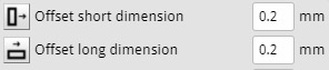
Offset
Type the value in mm for the offset and press Enter or click the corresponding Offset button.
Positive values will offset paste pads to the right or top. Negative values will offset the paste pads to the left or bottom.
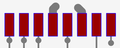
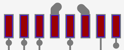
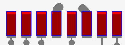
If you also selected the corresponding copper layer as extra layer, if the Solder Paste data that overlaps with the copper data will be shown in dark red otherwise, it is shown in bright red.
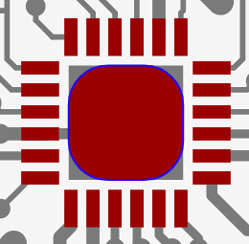
Enlarge/Shrink
You can enlarge or shrink any selected paste pads by an absolute dimension value. Type the value in mm and press Enter or click the Enlarge/Shrink button.
Positive values will add the given dimension to all sides of the selected pads. Negative values will reduce the size of the selected pads on all sides by the given value.
Resize
You can resize any selected paste pads by an absolute dimension value.

Type the dimension in mm and press Enter or click the corresponding Resize button.
Positive values will enlarge the size of the pad by the dimension entered and negative values will reduce the size of the pad by the dimension entered. Pads are resized from both sides, so the center of the pad remains unchanged.
Scale
If the Solder Paste opening will result in too much Solder Paste being deposited the a scaled reduction of the aperture opening is required on selected areas. In this case you can scale various sized paste pads to make them smaller by a given percentage.
Type the value for the scale and press Enter or click the Scale button.

The value is the percentage of the new surface area compared to the original surface area, so a value of 90 will reduce the pad to 90 percent of its surface area. Scaling is performed from all sides while the centre of the pad remains unchanged.
The scale value cannot result in paste pads of less than 50% of their original size.
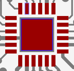
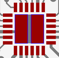
Split
Another way to reduce the Solder Paste surface area is to split the paste pad into smaller pads and can be achieved by using the split function.
This function will split the paste pad in 2 by adding a gap of the given size in the center of the original pad.
Type the value of the gap in mm and press Enter or click the corresponding Split button.

The gap value should be a positive value and cannot be more than half of the size of the original pad.
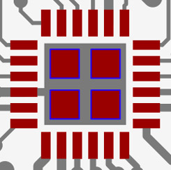
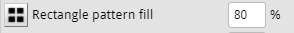
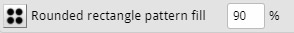
Pattern fill
In some cases you need to further optimise the paste surface. For larger surfaces it is sometimes better to fill the surface with a pattern of smaller shapes.
This can be done manually using the editing tools described above. However, we have developed an automated pattern fill function which will generate an optimised pattern according to your scale value.
This pattern fill function will split the original pad in either rectangles or rounded rectangles taking into account the minimum distance between 2 paste pads in order to still have enough remaining stencil material so the stencil remains stable as very thin parts of stencil material may bend or break during operation.
Type the value for the scale and press Enter or click the corresponding Pattern fill button.
The value is the percentage of the new surface area compared to the original surface area, a value of 90 will reduce the pad to 90 percent of its original surface area.
The algorithm will either reduce the size of the pad, or split the pad in multiple pads with a stable gap in between.


Back to Top