The Buildup Editor is a smart tool within the Visualizer which contains all our manufacturing capabilities and offers you price guidance to help you to define a cost effective buildup (or stackup) for your PCB.

To open the Buildup Editor click on either of the two ‘Buildup Editor’ buttons available in the PCB Configurator (center section of the PCB Visualizer).

PCB-Configurator-Buildup-Editor-Buttons

This will open in a popup window in one of two different modes depending on whether PCB data is uploaded or not:

  • No PCB data uploaded or data uploaded with basic analysis.
  • PCB data uploaded and full analysis is completed.

Buildup Editor No Data or with Basic Analysis

The Buildup Editor is available when no data has been uploaded or when only a basic analysis has been run.

When it opens there will 3 sections available as below:

  • Material – for selecting the number of layers, base material and board thickness etc.
  • Buildup – a graphical representation of the chosen buildup.
  • Available buildups – shows the available predefined buildups that can be selected.

Buildup-Editor-No-Data

NOTE


  • When you have completed all your changes please click on the ‘Apply’ button at the bottom of the window, this will close the editor and update the information in the PCB Configurator.
  • If you do not wish to keep the changes then click on the ‘Cancel’ button next to the ‘Apply’ button, this will close the editor and discard any changes you have made.

Material Section

This section allows you to select the materials and configuration used for the buildup of your PCB and you can change the parameters which will be reflected graphically in the Buildup section.

Buildup-Editor-Materials-Section

NOTE


  • If gold coins are displayed next to a parameter then this is an indication that the selected parameter will increase the cost of the PCB.
  • One coin stands for a small price increase but the selection stays poolable technology. A stack of coins stands for a non-poolable technology and thus a higher cost as we need to manufacture production panels filled with just this PCB.

Number of layers

Select the number of copper layers of the PCB

Board thickness

This represents the required nominal thickness of the PCB.

See also: Understanding Manufacturing Tolerances – Finished PCB Thickness Tolerance

Reversed buildup

A normal buildup uses cores for the internal layers and prepreg covered in copper foil for the outer layers. Whereas, a reversed buildup uses cores for both inner and outer layers with prepreg between the cores.

Buildup-Editor-Standard-Buildup

Standard Buildup

Buildup-Editor-Reverse-Buildup

Reverse Buildup

Base material

Select the type of base material (from the dropdown list) to be used in the construction of your PCB.

The type of material available will depend on the service selected in the PCB Configurator (PCB Proto, STANDARD pool, DEFINED IMPEDANCE pool, RF Pool, etc.).

See also:

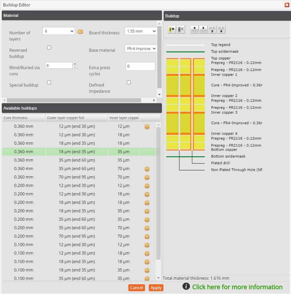
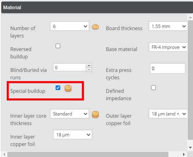
Blind/Buried via runs

Blind and buried vias require additional manufacturing ‘runs’ as part of a sequential buildup.

If your design requires Blind or Buried vias then use this option to add them.

Adding Blind or Buried via runs

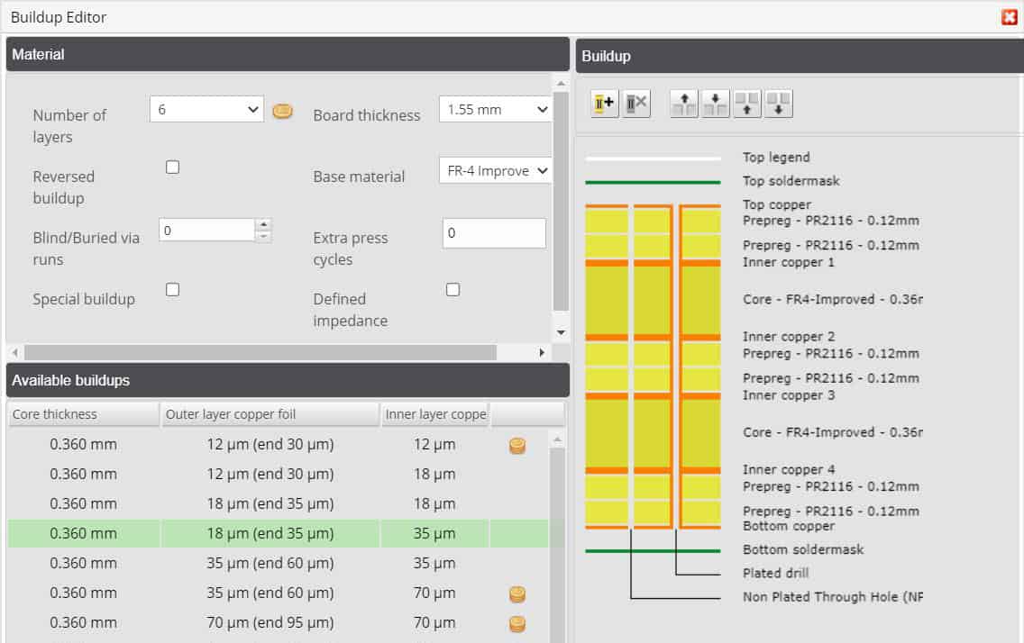
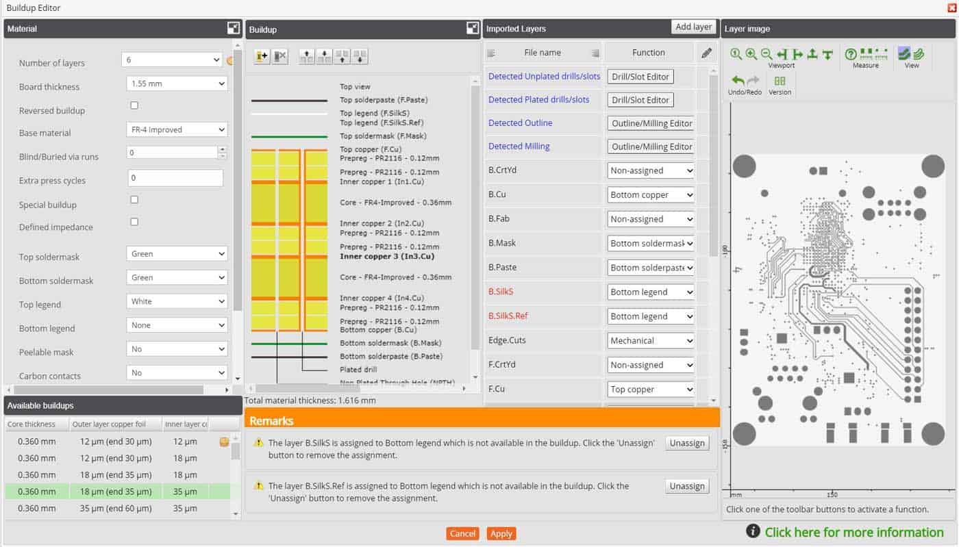
Select this option by clicking on the up arrow or by clicking on the ‘Add via’ button in the buildup section as below.

Buildup-Editor-Adding-Blind-Buried-Vias

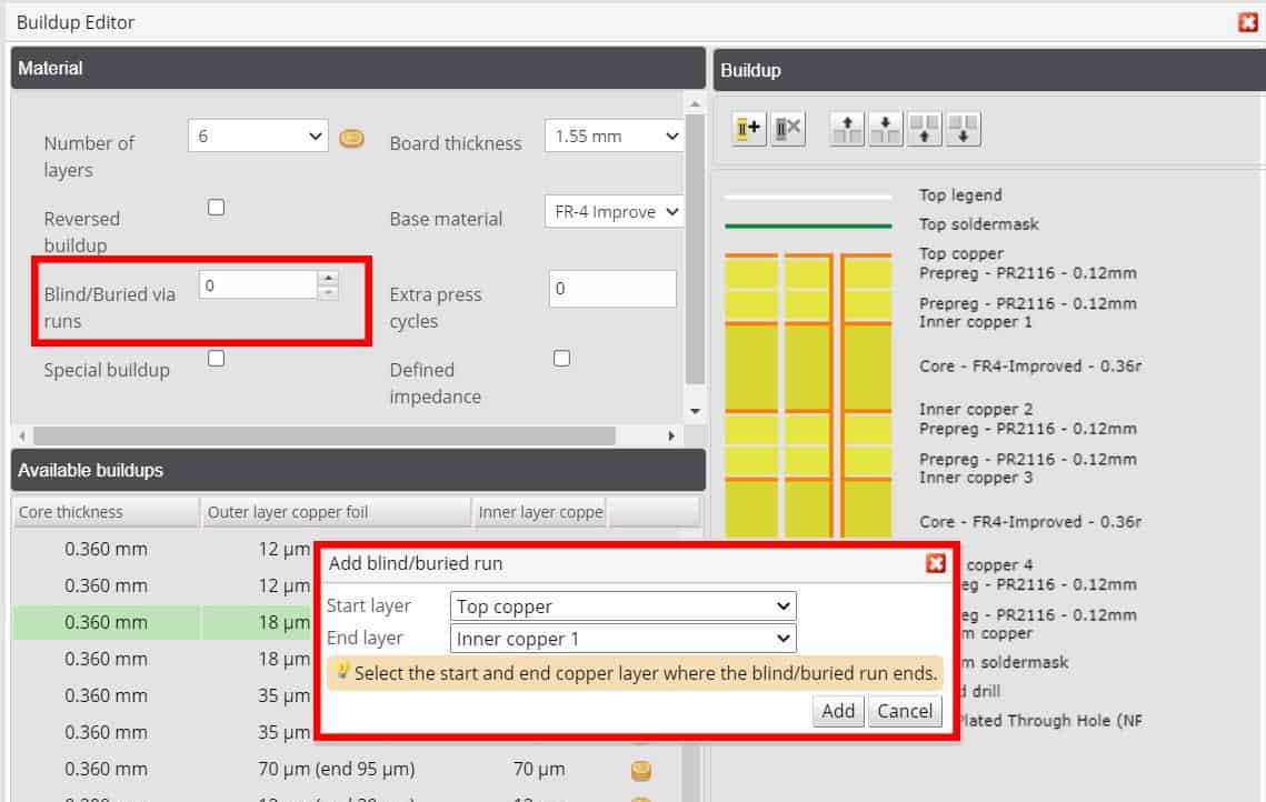
A popup will open where you can define on which layer the via starts and ends and click on the ‘Add’ button.

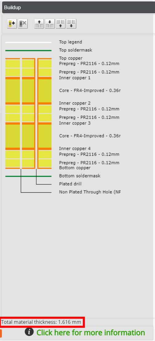
This will then update the image in the Buildup section showing the blind or buried via run added.

Buildup-Editor-Blind-Buried-Vias-added

To add more runs click on the up arrow or the ‘Add via’ button again.

Removing Blind Buried via runs 

If you wish to remove a run click on the down arrow or the ‘Remove via’ button and select which run to select from the popup and click on the ‘Remove’ button.

Buildup-Editor-Deleting-Blind-Buried-Vias

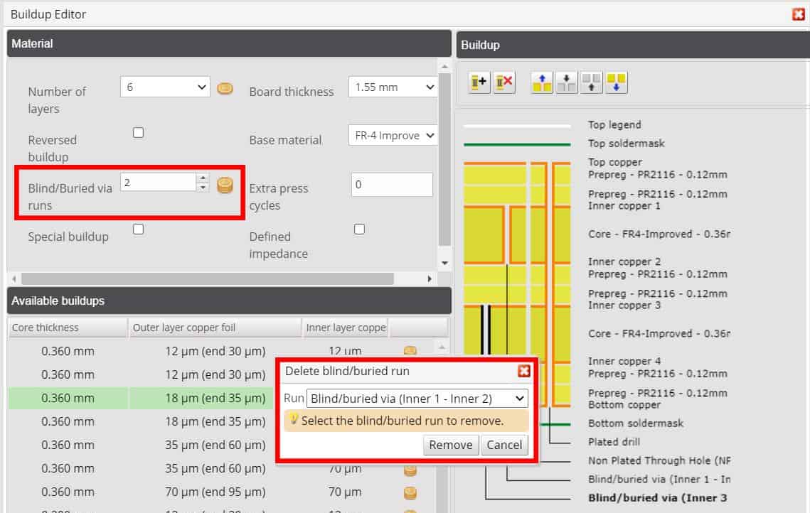
The run will be removed from the Buildup section.

NOTE


  • A Via must always go through an even number of copper layers.
  • Vias cannot end at the top side of a core.
  • Vias cannot start at the bottom side of a core.
  • Blind or Buried Vias cannot start or end inside or at the end of another Blind/Buried via unless the one is completely enclosed within the other (this will add extra cost as an extra press cycle is required).


See also:

Extra press cycles (non-editable)

This parameter indicates how many extra pressing cycles the buildup goes through as part of the sequential buildup described above.

It’s displayed for information purposes only and is an non-editable parameter.

Defined Impedance

Choosing this option will show only the available buildups for a DEFINED IMPEDANCE service.

It will also reveal an icon link to our Impedance Calculator.

Buildup-Editor-Impedence-calc-icon

The service in the PCB Configurator view will change to DEFINED IMPEDANCE’ when the ‘Apply’ button is clicked.

Impedance Calculators (Blog)

Special buildup

A Special buildup is one that is not in our standard buildups as displayed in the Buildup section.

When selecting this option 3 additional parameters become available and can be changed:

  • Inner layer core thickness.
  • Outer layer copper foil (start thickness)
  • Inner layer copper foil (start thickness)

Buildup-Editor-Special-Build

To change any of these 3 parameters click on the down arrow and select the required parameter from the available list to meet your requirements.

Available Buildup Section

We have over 940 predefined standard buildups available.

The buildup section displays all the available standard buildups for the parameters you have selected in the PCB Configurator and/or in the Materials Section.

To select one of the standard buildups simply click on it.

You will see the image in the Buildup section change to show a graphical representation of the selected build.

Click on the ‘Apply’ button and this will applied and the editor closed bringing you back to the PCB Configurator.

There are 3 columns in this section.

  • Core thickness – This is the thickness of the individual cores in the buildup.
  • Outer layer copper foil – This shows the start and final thickness of the outer layer copper.
  • Inner layer copper foil – This shows the thickness of the inner layer copper.

Coins that are displayed on the far right-most of some buildups indicates that this buildup will increase the price of the PCB.

The most cost-effective buildups are those without any coins.

Buildup-Editor-Standard-Buildup

See also:

Buildup Section

This provides a graphical representation of the elected buildup based on the parameters selected in the PCB Configurator and/or the Buildup Editor.

The nominal total material thickness of the PCB is shown in the at the bottom of this section.

Buildup-Editor-Total-Material-Thickness

IMPORTANT


  • To save any changes in the Buildup Editor click on the ‘Apply’ button.
  • This will close the editor and update the parameters in the PCB Configurator and if necessary the price.

Buildup Editor with Data Uploaded and Full Analysis

To open the BuildUp Editor is the same method with or without data being uploaded.

If you have uploaded your data and run the full analysis (only available when saved to your Shopping basket) then when you open the editor it looks different.

The main difference is that now the Buildup Editor is combined with the Layer Editor as below.

Buildup-Editor-with-Layer-Editor

To learn more please our Layer Editor User Guide.

Save Changes

To save any changes that you have made first click on the “Apply” button at the bottom of the Buildup Editors window, this will apply changes and close the Buildup Editor.

Next either select the “Summary” tab or the “Proceed to Summary” button, this will open the “Summary tab” then click the “Save changes” button.

Summary-Save-Changes