Introduction

The PCB Checker is part of the PCB Visualizer and allows you to verify the data uploaded and easily view any DRC (Design Rule Check) or DFM (Design For Manufacture) issues found during the analysis of the data.

IMPORTANT

The PCB Checker is only available after full analysis of the data has been completed and saved to the Shopping basket in your customer account. For more information, please see our How to Upload PCB Data User Guide.

DRC information vs DFM information

DRC information shows the results of the Full Analysis measurements against values set in the PCB Configurator (track width, isolation, annular ring etc.) and allows you to view any differences found one-by-one.

DFM information, also available after Full Analyses, shows information related to the PCB production process and relevant information for the Assembly process (Plating Index value, Copper surface (dm2) per layer, Solderpaste surface and Copper free of Soldermask, None connected pads free of soldermask that can be used as fiducial).

To view the DFM information simply click the DFM information tab in the DRC – DFM information section.

PCB Checker DRC & DFM Tabs

Opening the PCB Checker

Firstly, Sign in to your Eurocircuits User Account.

From the Shopping basket select the job you want to review and open the PCB Visualizer.

Shopping Basket Select Job

NOTE
  • If there is a red flag (Red Flag) in the PCB Visualizer column, then there are  DRC or DFM issues that require your attention.

The PCB Visualizer will open and next select the PCB Checker button from the tool menu at the top.

Select PCB Checker Tab

The PCB Checker will open showing the DRC information.

PCB Checker Opening Screen

Reviewing the DRC information

To review an issue, simply select the row in the DRC – DFM information section where the Measured value is shown in Red, this will highlight the row in Green as below.

PCB Checker DRC & DFM information section

Use the scroll bar on the right-hand side to scroll up and down.

The columns in this section are:

  • Layer – This is the functional name of the layer as defined in the Buildup Editor.
  • Required – The minimum value set in the PCB Configurator.
  • Measured – The minimum value measured during Full Analysis.
    • If this is smaller than the Required value, it is displayed in Red.
  • Red FlagRed Flag – Critical DRC issues which need to be resolved.
  • yellow remark TriangleWarning Triangle – Non-critical DRC issues.
  • SpannerOrange Spanner – DRC errors which can be auto-repaired.

On selection in the Birds Eye View and Detailed View sections the first instance of this issue will be displayed in Orange and all other instances will be displayed in Red.

This allows you to see the issue and its location on the PCB so that can assess what action is required.

PCB Checker Birds Eye and Detailed View

In the Detailed View you can zoom in & out using the mouse scroll button or the Zoom buttons at the top in the Viewport section.

To pan in all directions by clicking and holding in the left mouse button in the window and moving the mouse around or by using the Pan buttons (only X & Y) at the top in the Viewport section.

The Fault view will provide details of the issue and allow you to move to the next instance of this issue.

PCB Checker Fault view section

Resolving DRC Issues

Once you have reviewed the issue(s) there are several ways to resolve them depending upon what caused the issue.

Difference between Measured and Required Value

If the minimum measured value is less than the minimum value set in the PCB Configurator you can either:

There are 2 ways to change the minimum value set in the PCB Configurator:

Change the minimum value in the Related order details section of the PCB Checker by simply selecting the correct value from the drop-down list.

PCB Checker Related order details section

Alternatively, you can change the minimum value directly in the PCB Configurator.

IMPORTANT

This is a global setting for this specific feature (track width, isolation, annular ring etc).

Reducing the minimum value may affect the price.

or

IMPORTANT

Changing the CAD data may affect the price.

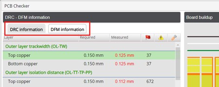
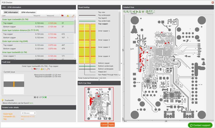
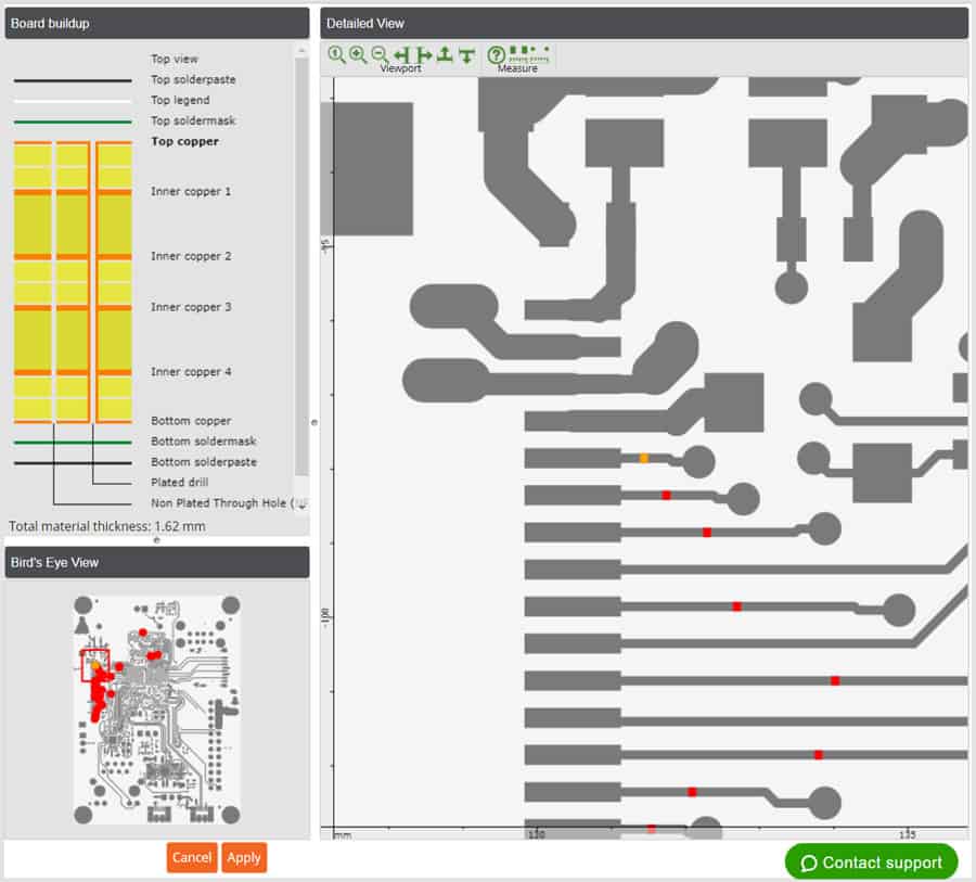
Reviewing the DFM information

In the PCB Checker select the DFM information tab.

PCB Checker DFM information Tab

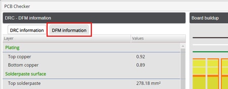
Here you will be able to review the results in the way as in the DRC information.

PCB Checker Birds Eye and Detailed View

The DFM topics we have introduced have the following purpose:

Plating index

This value is for top and bottom layers representing an estimate for the plating complexity.

This solely depends on the layout of the board and how evenly the copper is distributed over the individual outer layers.

A very low plating index (<0.4 and below) means that the layout will be difficult if not impossible to plate. See also: What is the plating Index?

Plating Index Solution

The Influence of Copper Distribution on PCB Quality

Solder Paste Surface

This value in combination with the thickness of the solder paste screen gives an indication of solder paste consumption per PCB.

Useful for the assembly process.

Non-connected soldermask free pads

Copper pads free of soldermask that are not connected to anything may be used as fiducials for further downstream processes such as assembly or testing etc.

Copper free of soldermask

This is the amount of copper (%) that is not covered by soldermask where no solder paste will be applied.

Eurocircuits uses this information as part of the calculation for the total area to be plated with the selected Surface finish (HAL Lead-free, Che Ni/Au, Che Ag etc.).

See also:

Selecting the Right Surface Finish for your PCB

Copper surface per layer

Provides an indication of the copper balance on each of the copper layers of the PCB.

If there is an imbalance of copper from layer to layer then this can result in bow and twist issues.

See also:

Understanding Bow and Twist on a PCB